

LITE: Capacity Crunch — What Moats Are Left for the All‑Round Pick‑and‑Shovel Player?
 I'm LongbridgeAI, I can summarize articles.
In 'From optical interconnect veteran to 'all‑round water seller': what makes Lumentum stand out?', Dolphin Research broke down Lumentum’s two core optical device lines. EML underpins the profit base in pluggable optics, while high‑power discrete lasers (UHP CW) are a bet on the next‑gen CPO/NPO architectures. $Lumentum(LITE.US)
The underlying logic converges on one point. With severe supply‑demand mismatch in high‑end laser chips and scarce in‑house capacity, leading vendors are simultaneously benefiting from pricing power, LTAs and margin expansion.
But both EML and CW must be 'cut' from the same indium phosphide (InP) wafers. InP crystal growth is slow, there are no foundries, and new capacity takes 2–3 years to ramp, which means Lumentum’s growth will eventually hit a wafer capacity ceiling. So what other cards does Lumentum hold?
We continue the discussion here and focus on two questions:
- Why does Scale‑across give legacy telecom devices a new lease on life?
2) Why is Lumentum entering the lower‑margin module biz.?
I. Other telecom devices & industrial: Scale‑across gives 'old trees new blossoms'
Lumentum’s telecom biz. has been a classic stock‑driven market in recent years. Demand comes from global carriers with steady capex cycles and growth tied to network expansions. This AI wave breaks that narrative for a simple reason: power is not enough.
A single data center campus has a cap on available power. Once training clusters exceed what one campus can supply, jobs must run across campuses, with another DC tens to hundreds of kilometers away operating as if it were the same machine as the local hall. That inter‑campus fabric is Scale‑across.
As distance increases, intra‑DC optical interconnects fail to hold up.
Within a DC (Scale‑up & Scale‑out), IM‑DD is widely used, carrying data via optical intensity and using photodiodes for direct detection to convert light into electrical signals. This approach is low cost and low power, but the drawback is it captures only intensity at the receiver, losing the optical phase information during O/E conversion.
Over short distances the impact is limited and can be mitigated by DSP in the electrical domain. Over long fiber spans, chromatic dispersion causes different wavelengths to propagate at different speeds, broadening pulses and ultimately creating inter‑symbol interference.
Therefore, inter‑campus and long‑haul links must adopt coherent optics and encode via phase and polarization. On the receive side, a local oscillator mixes with the signal for demodulation to recover amplitude and phase, while a coherent DSP handles dispersion, nonlinear impairments and FEC.
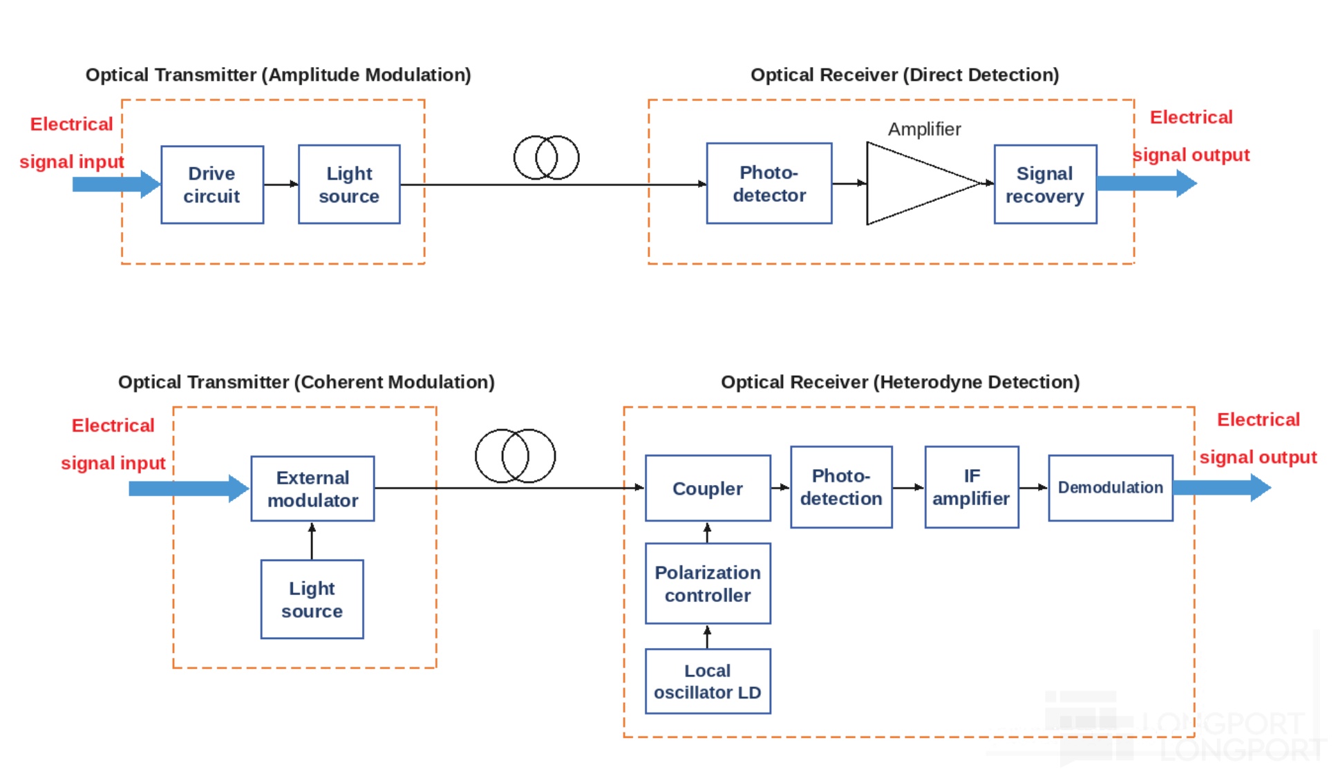
(Note: upper diagram shows IM‑DD with direct laser modulation. The lower diagram shows coherent links, where the receiver adds a local oscillator, mixes with the received signal, then extracts amplitude and phase.)
However, coherent solutions materially increase system complexity. They require ultra‑narrow‑linewidth tunable lasers, high‑precision coherent modulators, dual‑pol receivers, and EDFAs every few tens of kilometers to compensate for optical power loss.
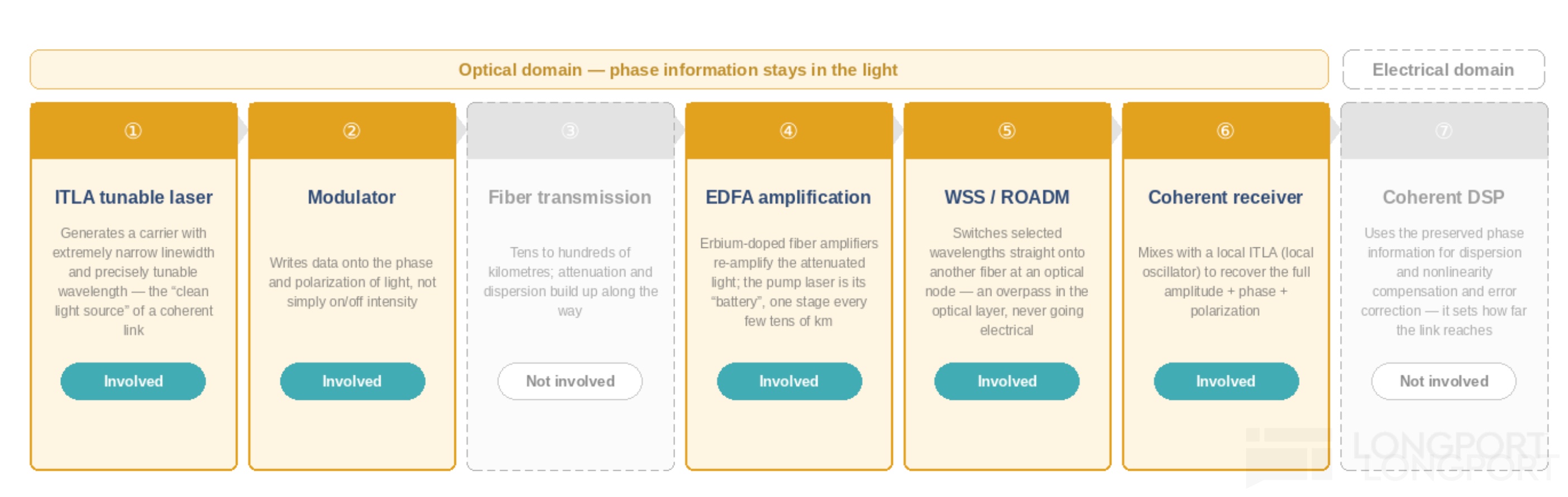
For Lumentum, its coherent photonics know‑how in long‑haul and metro networks, plus transmission engineering capability, can be repurposed for AI DCI Scale‑across. The same applies to inter‑campus links.
Below, we discuss two representative components in coherent links where Lumentum is strong.
1) ITLA — the 'clean' light source for coherent links
ITLA (integrable tunable laser assembly) is the light source inside a coherent module, with a single job: provide a continuous, 'clean' laser output. A ZR module typically has one ITLA; its output is split, with one path modulated and transmitted, and the other retained locally as the LO for coherent demodulation. If the source quality falters, both Tx and Rx suffer.
'Clean' means meeting three criteria.
a) Ultra‑narrow linewidth: color is determined by wavelength, and even a 'single‑color' laser spreads slightly around a center wavelength. That spread is the linewidth.
Narrow linewidth ensures phase coherence over time. Since information is carried in phase, if the source phase jitters, the receiver cannot distinguish data from noise.
b) Precise tuning across the C‑band (the 1310/1550 nm comms bands have minimal fiber loss) to any channel. c) Long‑term stability of source quality.
Unlike EMLs (where each speed grade needs a new modulator design and complex epitaxy), ITLA’s challenge is not the chip architecture itself, which does not need redesign with data rate upgrades. After two decades of iterations, chip and cavity designs are mature.
The core manufacturing difficulty lies in micro‑packaging and full‑band calibration. These steps determine whether an ITLA can deliver the 'clean' light required for coherent comms.
a) Micro‑packaging: as noted earlier, EML/CW optics are essentially linear chains — chip output couples via lenses/isolators into fiber, with wavelength fixed by the chip and set at factory, and optics arranged in series one‑to‑one. The path is straightforward.
By contrast, ITLA adds a feedback loop for self‑correction. A small fraction of the output is tapped and fed to a wavelength locker, which compares the current wavelength to a standard grid and feeds back to adjust drive current.
Thus, ITLA packaging is not just about protecting the chip and extracting light. Without highly integrated optics, each discrete element — lenses, isolators, prisms, etalons — must be placed and angled with micron precision, bonded, sealed, temperature‑controlled, and connected for power and fiber.
This added feedback path introduces a set of optics requiring micron‑level alignment that must not drift under temperature swings and long‑term aging. That raises packaging difficulty materially.
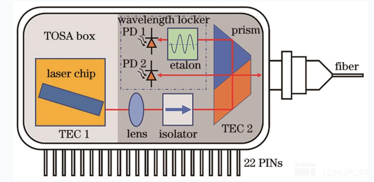
Source: Acta Optica Sinica (ITLA schematic)
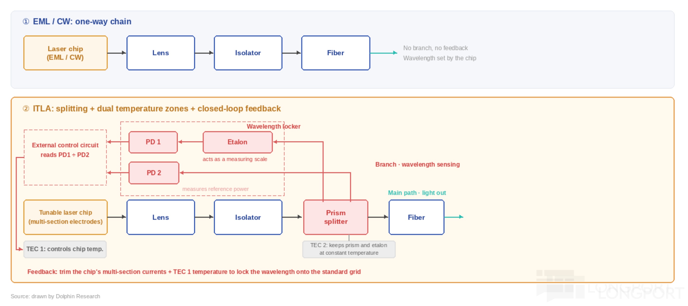
b) Full‑band calibration: EML/CW operate at a single fixed wavelength, so calibration is simple — set drive current, output power, ER, etc., at a target temperature, and you are done. The process is single‑point.
Coherent transmission uses DWDM, where dozens of channels co‑exist in a single fiber, each at its own wavelength and separated by tight spacing. Hence, ITLAs must tune anywhere within the C‑band and switch under command across tens of channels, up to nearly one hundred.
To lock a channel stably, one must co‑tune the reflector and phase sections (via current or heater power), the gain section current, and chip temperature. These variables are coupled and non‑linear with respect to output wavelength, so there is no one‑size‑fits‑all lookup table.
Therefore, every ITLA requires per‑unit full‑parameter calibration before shipment. Over the full operating temperature range, the system sweeps combinations of control variables, records the resulting wavelength and power, and writes a multidimensional 'control‑to‑wavelength' map into memory. The precision of this map determines first‑time lock success during channel switching.
Insufficient calibration precision causes wavelength offsets during switching and can induce crosstalk. This is a critical yield and reliability factor.
Overall, the two bottlenecks — micro‑packaging and full‑band calibration — hinge on manufacturing and test engineering rather than chip design or materials. The gaps show up in yield, long‑term stability, and model accuracy, and can theoretically improve with scale.
As a result, there are multiple players. Overseas vendors include Lumentum, Coherent, Sumitomo Electric and Fujitsu, while in China the Huawei ecosystem and Accelink have self‑developed ITLAs mainly serving domestic carrier networks.
For Lumentum, the key edge is long‑standing qualifications within overseas OEM supply chains. Most domestic vendors’ reliability data are accumulated on Chinese networks and have limited acceptance abroad, but as coherent pluggables gain share and Chinese vendors progress through overseas certifications, we expect Lumentum’s qualification moat to narrow.
2) Pump lasers — the 'excitation source' feeding EDFAs
Coherent signals attenuate along fiber spans. Think of it as a car on a long trip, burning fuel as it goes and needing gas stations and tankers along the route.
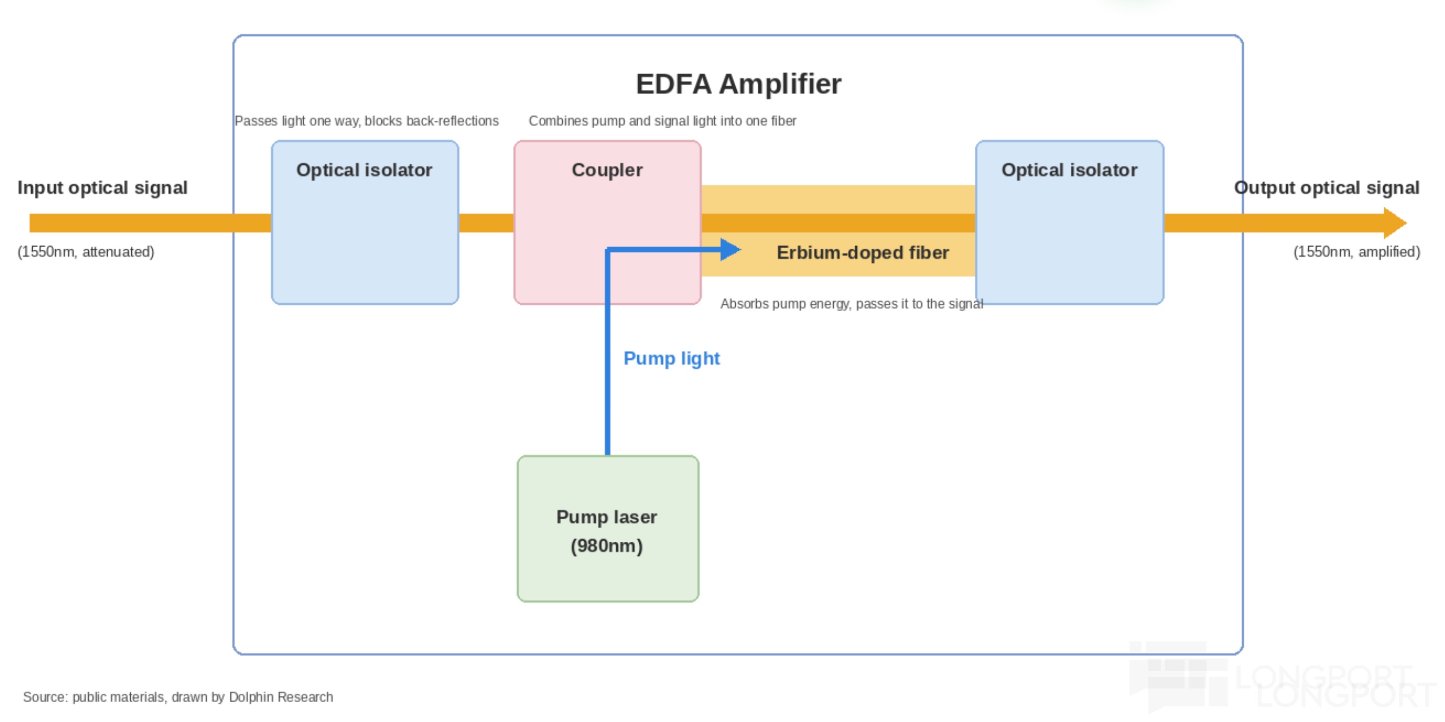
EDFAs — erbium‑doped fiber amplifiers — are the gas stations. Pump lasers are the tankers, injecting pump light into the erbium‑doped fiber, where erbium ions absorb it and store energy.
When the C‑band signal passes, these energized erbium ions are stimulated to emit light identical to the signal, thus amplifying it. The 980 nm pump is an energy source, not a data carrier, so spectral purity is less critical, but output power is key.
Lasers emit light when electrons drop from higher to lower energy levels and release photons, with larger bandgaps yielding higher energy. The bandgap depends on the semiconductor material system.
The active layers are grown epitaxially over the substrate, and the substrate largely dictates material systems and achievable wavelengths. EML, ITLA and CW for C‑band use InP substrates.
But 980 nm pumps — EDFAs absorb 980 nm or 1480 nm, with long‑haul using 980 nm — require GaAs‑based materials. The substrate choice is fundamental here.
With that materials divide in mind, consider the core barriers in pump lasers.
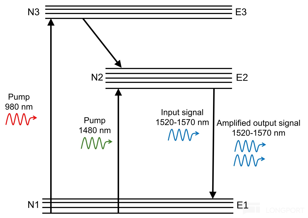
Source: Optica.ca, erbium energy level diagram for EDFAs
After polishing, epitaxy and chip processing, optical chips are not sawn like silicon photonics. They are cleaved along crystal planes to achieve atomically flat facets, a step known as chip cleaving in production.
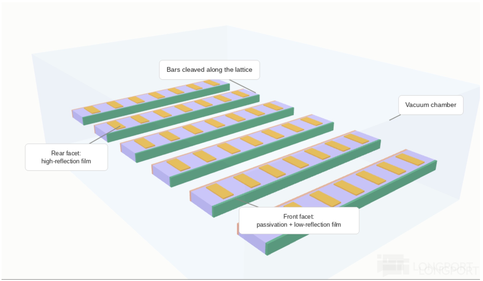
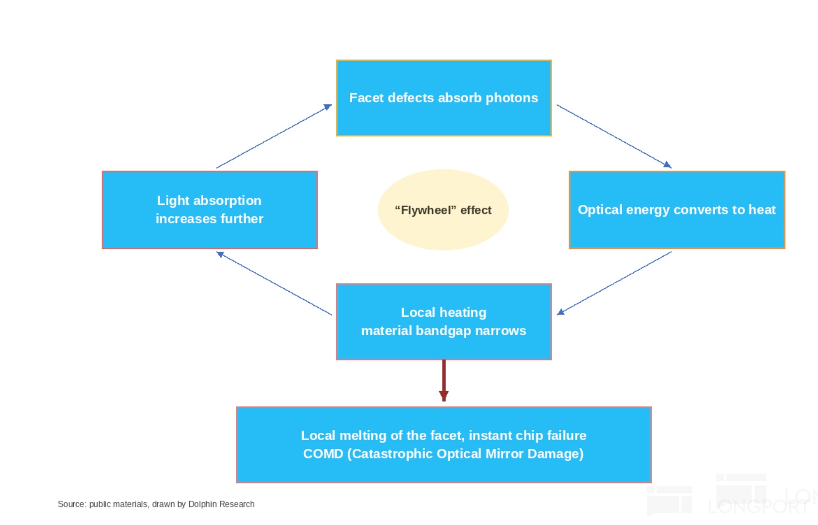
The craft lies in the exposed laser facets after cleaving. Two issues arise immediately after 'breaking' the chip open.
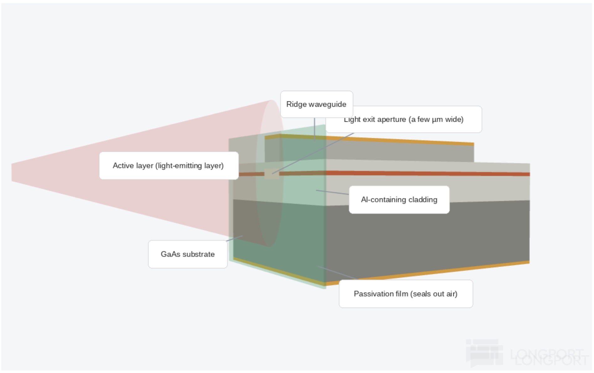
a) 980 nm pumps deliver high optical power through a small aperture, imposing high power density on the facet, which is prone to damage. b) With GaAs substrates, gallium is more reactive, and adding aluminum in the epitaxy accelerates oxidation at the exposed facet.
Oxidation increases absorption, generates heat, and causes local facet melting, destroying the laser — the so‑called COMD (catastrophic optical mirror damage). This is a key failure mode.
The solution is facet passivation: in an ultra‑high vacuum, deposit a protective film on the facet to prevent oxidation. The green layer below illustrates the passivation, which isolates the facet from air.
Unlike ITLA micro‑packaging — where equipment and optics can be sourced and the gap shows in assembly yield — facet passivation is materials/process know‑how. Film composition and thickness, vacuum conditions, and cleave‑to‑coat timing each determine the power threshold the facet can withstand.
Lumentum’s facet passivation is best‑in‑class. Beyond passivation, it employs internal non‑absorption windows to eliminate facet absorption and significantly raise the COMD threshold.
On competition, telecom‑grade 980 nm pumps with tight beam profile specs remain concentrated among a few overseas players: Lumentum (heritage tracing back to SDL), Coherent and Furukawa Electric. Per management, Lumentum’s market share is around 70–80%, implying a highly concentrated market.
Beyond these two highlights, the table below maps Lumentum’s coherent product lineup and key competitors. It shows the scope of the portfolio.
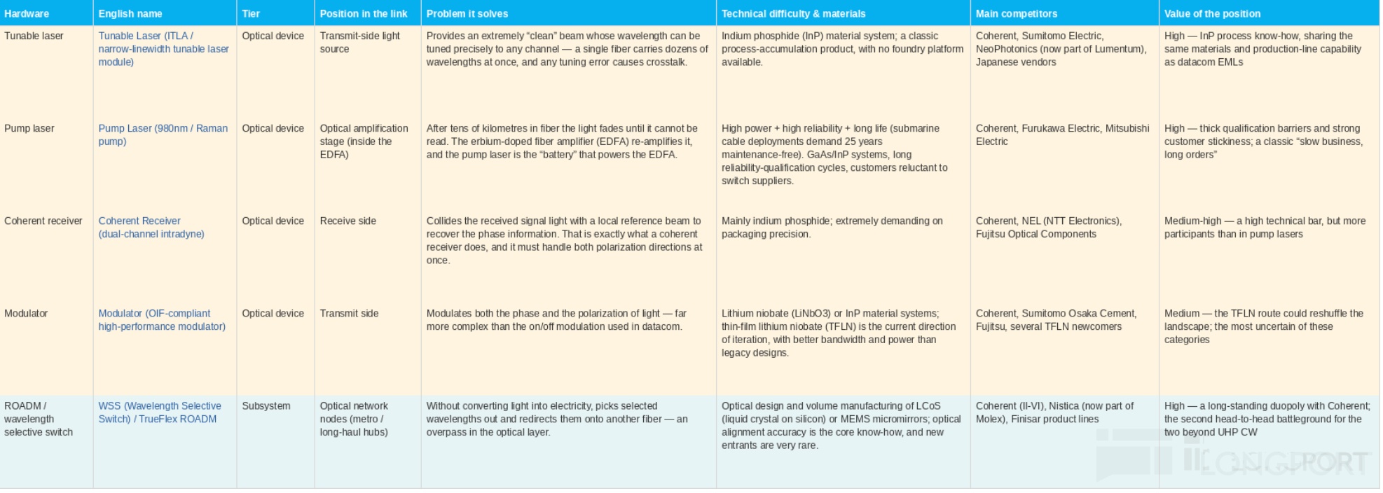
A clear pattern emerges. The closer one gets to fundamental light physics — emission and amplification — the higher the market concentration, as these rely on compound semiconductor epitaxy and chip processes with higher barriers.
Moving up toward modulators and systems, competition becomes more diverse and complex. This bifurcation shapes strategy.
Overall, Lumentum selectively extends downstream only where it commands core light‑chip leadership. It integrates into modules or sub‑assemblies such as 800ZR/1.6T ZR coherent modules and Nano‑ITLA components, securing natural GPM and supply assurance advantages.
It avoids over‑committing in areas lacking light‑chip moats where it would face DSP giants like Broadcom and Marvell head‑on. That discipline matters.
Telecom revenue is about $1.2 bn, roughly 40% of company sales. Based on checks, the portion tied directly to AI Scale‑across DCI is around $300 mn (about 25%), with the remaining $900 mn tied to steady carrier demand.
Timing‑wise, DCI coherent pluggables are moving from today’s mass‑deployed 400ZR to 800ZR. This is the next step‑up.
Per Cignal AI, 800ZR should scale in 2026–2027, with 1.6T ZR entering commercialization from 2028 (the 1.6T ZR spec was released in Sep‑2026, with sampling in 2027 and volume from 2028). The value per light source will step up again.
Given current YoY shipment growth of 80–130% (pump lasers up over 80% YoY and narrow‑linewidth tunable lasers up 130% YoY in the latest quarter), AI Scale‑across will drive a second growth curve for legacy telecom devices. This creates a strong uplift.
The analysis above shows that EML as the profit base, CW including UHP‑CW as the incremental bet for compute clusters, and coherent DCI unlocked by AI Scale‑across all compete for the same constrained InP wafer capacity. The bottleneck is common.
For Lumentum, under InP wafer constraints, maximizing earnings elasticity requires either lifting value per wafer — prioritizing higher‑value chips to maximize revenue and profit per wafer — or opening new lines that do not consume InP wafers. That removes the capacity ceiling at the source.
We now turn to that:
4) Optical modules: from chips to modules, building full module‑level delivery
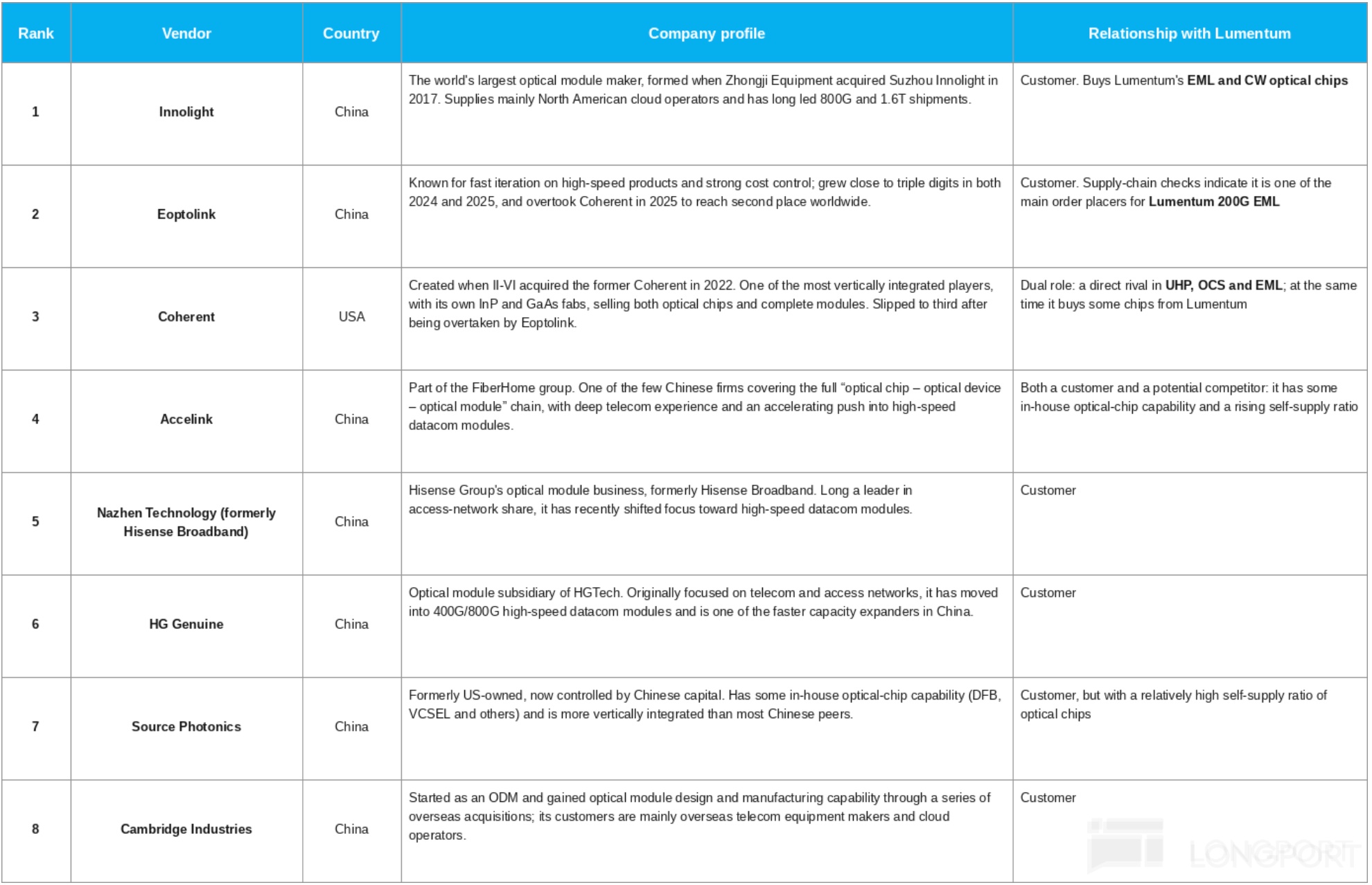
After acquiring Cloud Light in 2023, Lumentum gained the ability to deliver full 800G/1.6T pluggable modules directly to Google, AWS and other cloud providers. These serve Scale‑out inter‑rack links, with delivery moving up from light chips to full modules.
Competition is intense in pluggable modules, a mature and highly contested market. Per LightCounting, seven of the top ten global optical module vendors are from China.
Chinese vendors have clear advantages in capacity and manufacturing cost. Hence Lumentum does not chase volume and cost on standard SKU pluggables.
Instead, it focuses on customized, higher‑speed, higher‑barrier modules. This carve‑out aligns with its strengths.
Based on checks, Lumentum’s annual module revenue is around $720 mn, about 24% of total and the largest single product line. But GPM is only about 30%, well below device businesses discussed earlier.
If pluggables are crowded and margins thin, why buy Cloud Light? We see two core reasons.
a) In‑sourcing light sources to improve module profitability. Historically, Cloud Light bought lasers externally.
The company is now inserting its own CW sources into modules, with about 20% self‑supplied today and rising over time. Capturing light‑source value internally lifts module margins.
Given light sources are roughly 17–18% of module ASP, if self‑supply rises from 20% to 50%, module GPM could improve by around 3 ppt. This is a meaningful lever.
b) Completing module‑level packaging, system validation and cloud‑grade delivery credentials to pave the way for NPO/CPO. On earnings calls, management noted that some NPO/CPO customers require subsystem/full‑module delivery capability.
If a vendor only ships bare chips, even UHP‑CW meeting spec cannot directly win ELS system orders. Cloud Light’s packaging, system test, and cloud certifications close Lumentum’s capability loop from chip to full module.
This is effectively a ticket into the ELS system supply chain. It de‑risks downstream moves.
5) OCS optical circuit switches: a 'down‑shifted' adjacency
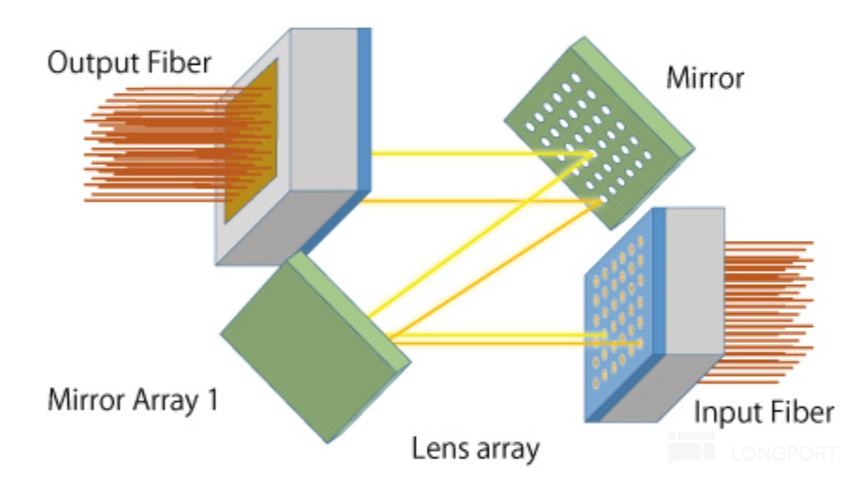
Finally, Lumentum’s OCS — a pure optical switch replacing SPINE‑layer electrical switches in DCs — delivers ultra‑low latency and transparent transport. Technical details are covered in this piece on Google’s 'optical network'.
Why OCS for Lumentum? It follows the same logic as DCI coherent devices — reuse of existing capabilities.
The MEMS chip with hundreds of micro‑mirrors is the same optical path steering technology used for two decades in telecom WSS. Both steer beams precisely to target ports via micro‑mirror deflection, though WSS routes by wavelength while OCS switches by physical ports.
Thus, when Google scaled OCS to replace electrical switches in TPU clusters and sought an external supplier, Lumentum was among the very few able to deliver hundreds‑of‑port OCS with a MEMS micro‑mirror engine proven in carrier networks over decades. This credibility matters.
Competition spans five routes: Lumentum’s 3D‑MEMS, Coherent’s LCOS (with limited DC commercial time so far), Polatis’ piezoelectric approach, iPronics’ silicon photonics (micro‑second switching but limited port scalability), and Telescent’s robotic fiber re‑patching. The landscape is still evolving.
So far, the OCS route has not converged, but only MEMS has met both hard requirements: hundreds of ports plus validation in hyperscale AI clusters. It has cleared Google TPU scale deployment.
Therefore, Lumentum’s OCS advantages are first‑mover status and large‑scale field validation. The fundamental principles are not a high barrier, with the key hurdles in manufacturing scale and cluster‑level engineering.
The biggest risk is customer concentration and potential competition. Google is both the largest OCS customer and a potential in‑house rival.
Further scale depends on whether a second wave — Microsoft, Meta and others — follows with volume deployments. As of now, only Google has scaled; Microsoft, Meta and AWS remain in small‑scale prototyping.
Wrap‑up: the only full‑stack 'water seller' in optical connectivity
Across these two articles, each shift in AI compute topology creates demand for Lumentum. The company is positioned across layers.
Scale‑out (inter‑rack): high‑end EML chips defend the ultra‑high‑margin base in pluggables. This remains the cash generator.
Scale‑up (intra‑rack): next‑gen CPO/NPO unlocks a surge via UHP CW chips. This is the growth engine.
Scale‑across (inter‑campus): power constraints drive distributed clusters, repurposing ITLA, pump lasers and ROADM/WSS from telecom into long‑haul DCI. This turns legacy assets into new growth.
Spine layer topology: MEMS‑based OCS targets all‑optical switching, opening a large, high‑margin second curve that does not consume InP wafers. This diversifies the constraint.
In short, regardless of which layer AI optical networks evolve along, Lumentum has indispensable positions at the base. In the next piece, we will model segment earnings and assess what Lumentum is worth. Stay tuned.
<End>
Dolphin Research optical interconnect series:
'AI in the hyper‑connected era: racing toward light?'
'Copper will not quit: CPO — real opportunity or mirage?'
'Challenging NVDA’s dominance: why Google’s 'optical network'?'
'From optical interconnect veteran to 'all‑round water seller': what makes Lumentum stand out?'
Risk disclosure and disclaimer: Dolphin Research disclaimer & general disclosure


The copyright of this article belongs to the original author/organization.
The views expressed herein are solely those of the author and do not reflect the stance of the platform. The content is intended for investment reference purposes only and shall not be considered as investment advice. Please contact us if you have any questions or suggestions regarding the content services provided by the platform.