

Cerebras: Wafer-scale 'monster' chip—can it challenge NVDA?
 I'm LongbridgeAI, I can summarize articles.
Most chip designers, including NVIDIA, etch circuits onto a large wafer, dice it into small dies, then interconnect those dies into an AI accelerator to avoid scrapping the whole wafer due to defects. One company chose a different path and refused to play it safe.
It directly treats the entire wafer as a single chip, roughly the size of a 21.5cm x 21.5cm square fruit tray (close to the max rectangle extractable from a 12-inch wafer), packing 4 trillion transistors and 900,000 active cores. That company is Cerebras.
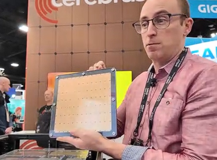
The GPU inference bottleneck is the 'memory wall'. NVIDIA keeps working around it,$Cerebras(CBRS.US) uses a wafer-scale chip to tear it down, and its moat sits outside TSMC in design, fault tolerance, and packaging.
This piece focuses on what WSE (Wafer Scale Engine) is, the GPU pain points it addresses, and how WSE is built and where the hard parts are. The next article will cover Cerebras’ operating performance and outlook.
I. What does Cerebras do?
Cerebras’ core product is the WSE (Wafer Scale Engine), named to distinguish it from conventional die-scale chips, as it is built at the wafer scale.
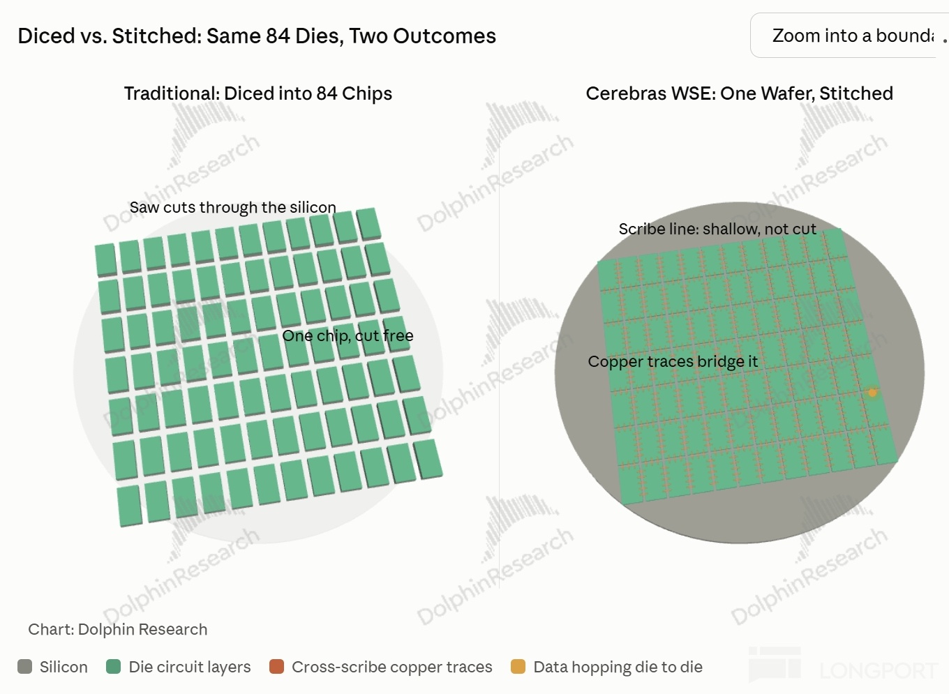
Peers typically dice a wafer into dozens or hundreds of stamp-sized dies (~800mm²), then stitch them back with high-speed interconnects to behave as one big accelerator. That is the standard approach.
Cerebras’ logic is: if you are going to stitch it back anyway, why cut it in the first place? It therefore etches the full range of compute on one intact wafer.
Cerebras partitions the wafer into a 12-by-7 grid of 84 identical tiles (dies), which are not independent chips. Neighboring tiles are interconnected, and the 84 tiles together form one single chip.
Each die holds 10.7k active cores, with each core just 0.05mm². One wafer (chip) thus has 900k active cores (about 970k physical cores with ~7% design redundancy to cover yield).
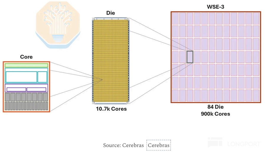
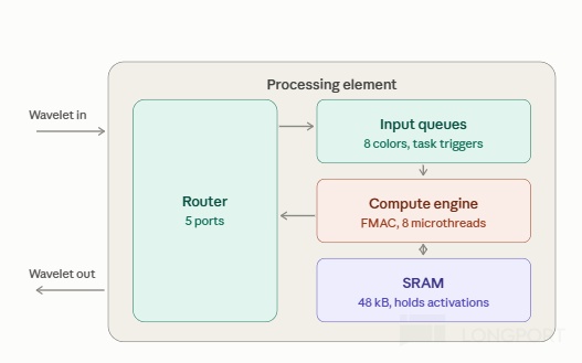
Zooming in, each core integrates three blocks: a router, a compute engine, and 48KB of SRAM (970k cores per wafer map to roughly 44GB of SRAM). Area is roughly split in half between logic and memory.
Under this fruit-tray-size chip model, Cerebras is the only WSE player, and because each WSE core is just 0.05mm² (vs. ~3mm² unit blocks at NVIDIA and Apple), the footprint is unique in the market. There is no second standard.
The compute core, router, and SRAM combo inside each WSE core are Cerebras’ own designs. Unlike HBM purchased from memory vendors, the SRAM bit-cell design and foundry work are done by TSMC and included in the wafer price.
In actual workloads, GPUs and WSE (Cerebras) differ mainly as follows:
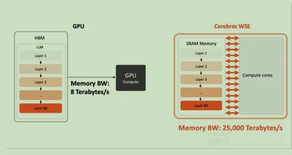
1) A GPU is a library. The full encyclopedia (weights) sits in the stacks (HBM), and hundreds of readers (SMs, the core compute units) sit in the reading room. To write a single character, every reader must flip the whole set again, and there is only one corridor from stacks to room that carries 8TB/s.
2) WSE (Cerebras) does not build a library. It hires 900k people (cores), each memorizing a tiny chunk of the encyclopedia. There is no stacks, no corridor, and no runners. To write a character, you read the question once, everyone immediately recalls their chunk, and you aggregate the answers.
Within a WSE core, the three blocks do the following:
i) SRAM: most capacity stores weights (that memorized page), with a small portion for activations, KV cache, etc. (scratch paper). It is the local memory bedrock.
ii) Compute unit: when a number (activation) arrives, it performs a multiply and an add; if nothing arrives, it idles and consumes negligible power.
iii) Router: distributes prompts and collects answers. It ‘reads the question to everyone’, aggregates responses, and forwards results to the next stage. That is its role.
Because of WSE’s construction, it tackles GPUs’ primary issue by slashing data transport time and breaking the memory wall.
On GPUs, weights live in HBM and must be moved in full for each token (B200/B300 bandwidth 8TB/s). On WSE, weights are pre-placed into SRAM next to the compute.
II. How GPUs fight the memory wall
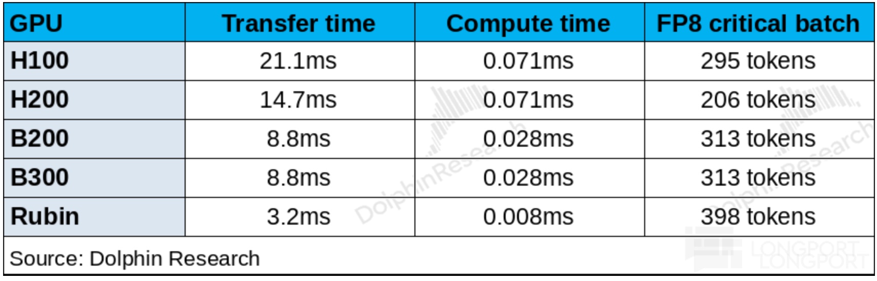
HBM transfer time dwarfs GPU compute time. Using Llama 70B (FP8) on a B300 reference, HBM transfer is ~8.8ms while GPU compute is just ~0.028ms, under 0.5% of transfer time.
That implies 99.5% of wall-clock goes to waiting for weights to move from HBM, idling GPU FLOPs and creating the key inference bottleneck. This is the crux of the problem.
Note: HBM transfer = 70B params x 1B/param ÷ 8TB/s = 8.8ms; GPU compute = 2 ops x 70B params ÷ 5 PFLOPS = 0.028ms.
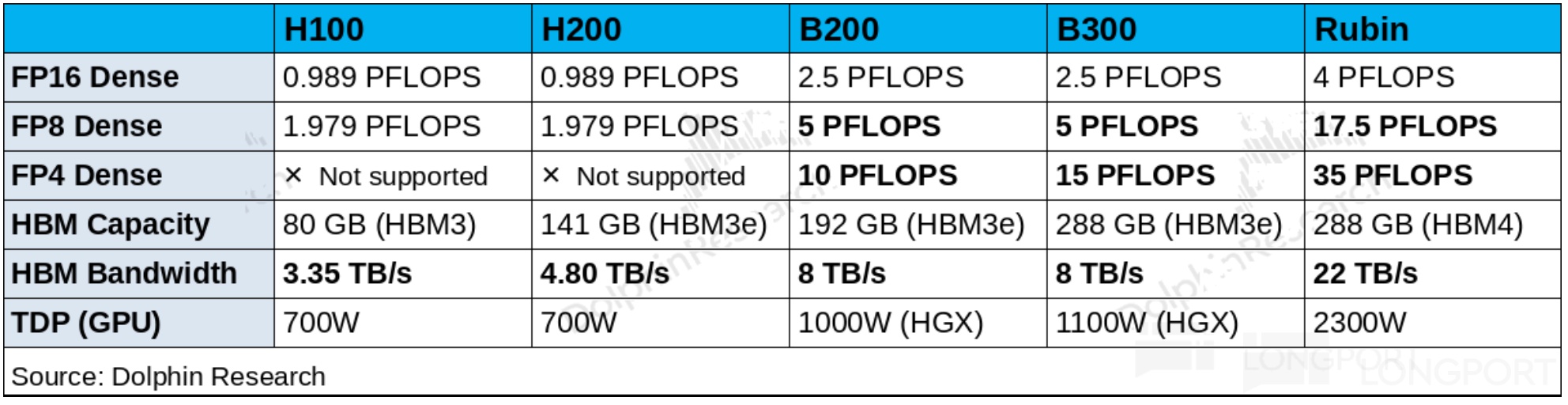
Across GPU generations, even if Rubin lifts HBM BW by 2.75x to 22TB/s, Rubin’s 17.5 PFLOPS compute is up 3.5x. Idle time still sits around 99.5%.
The main workaround is batching. Since everyone needs the same weights, once you pay the transfer cost, you might as well process many requests together (given 99.5% idle time, you can amortize the transfer).
The goal is to launch hundreds of compute tasks per transfer to amortize data movement. You can estimate the theoretical batch limit (313->398); below that, you waste compute, and above it, you waste bandwidth. That is the trade-off frontier.
Batching boosts GPU utilization and unit economics, but it creates client-side issues that hurt UX:
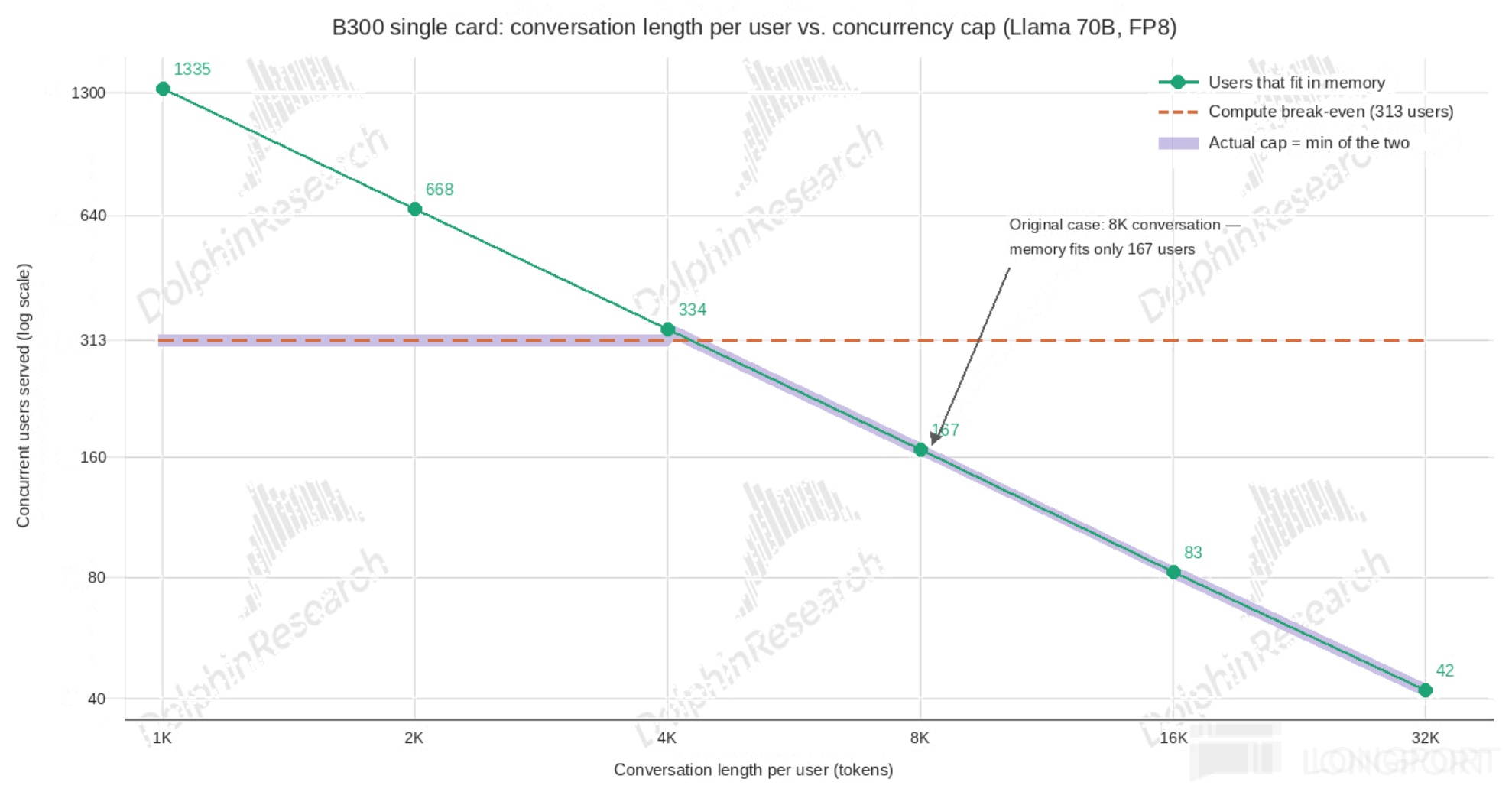
1) KV cache caps batch size: weights are shared, but each user’s conversation memory (KV cache) is private. In Llama 70B at FP8, each token needs ~160KB; with an 8k context, one user’s KV cache is ~1.3GB (8192 x 160KB).
On a B300 with 288GB HBM, after loading Llama 70B FP8 weights, ~217GB remain for KV cache. If one user needs 1.3GB, a single card serves 167 users with 8k contexts in parallel. That’s the ceiling.
Our prior batch threshold estimate was ~313, so the practical cap at ~167 is already binding. KV cache fills HBM and limits batching headroom. This becomes the new bottleneck.
2) The latency-throughput knot: while batching improves throughput (and provider unit costs), it increases first-token latency (waiting to form a batch) and inter-token latency (contention). Hence most GPU inference APIs offer ‘fast but pricey’ vs. ‘slow but cheaper’ tiers.
To mitigate batching pain, GPU vendors (NVIDIA) pursue several directions:
Approach 1: Scale from a single card to a rack to lift total HBM capacity (push out the KV cache ceiling). From H100 -> B300 -> VR200 racks, rack-scale HBM helps relax KV cache limits and improves batching efficiency.

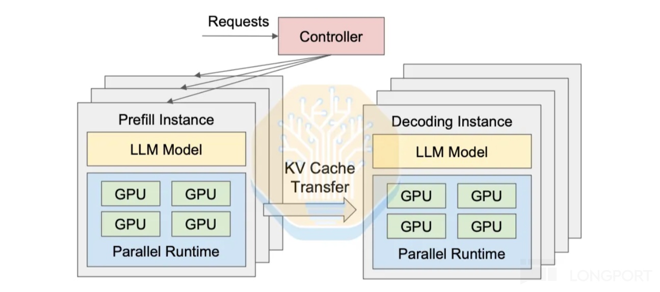
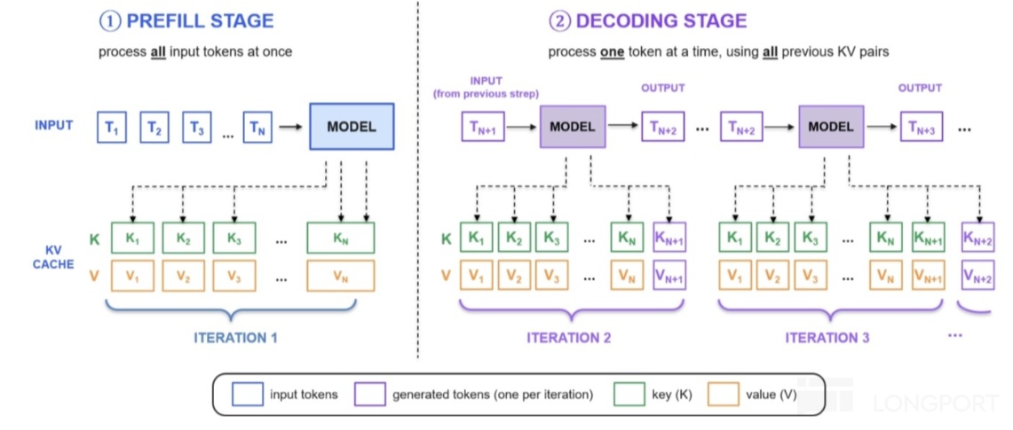
Approach 2: System-level disaggregation — Disaggregated Inference: split Prefill (build KV cache) and Decode (consume KV cache) into separate GPU clusters, connected by a KV cache pool.
a) Prefill: processes the full input context. It is compute-intensive and well-suited to GPUs. It sets up the working set.
b) Decode: predicts new tokens and is memory-bandwidth bound. It is latency-sensitive because the model generates tokens sequentially. This stage needs careful bandwidth allocation.
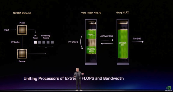
In the traditional GPU path, Attention and FFN contend for HBM bandwidth. After NVIDIA acquired Groq, the new VR200 architecture introduces LPX racks centered on Groq’s LPU and further splits Decode into Attention and FFN.
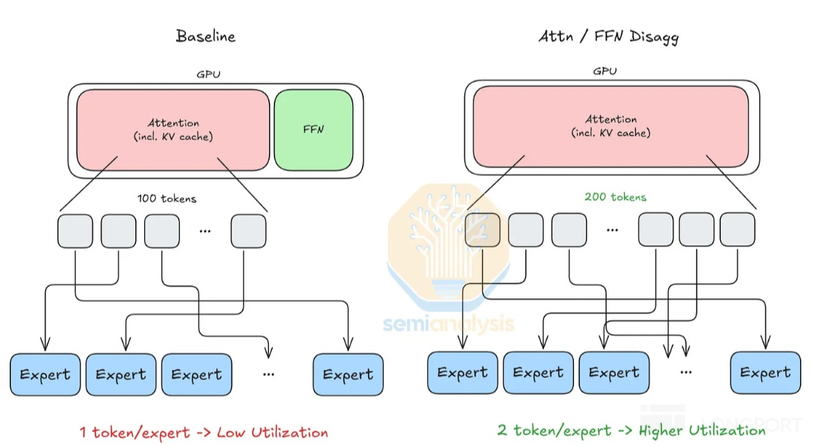
i) Attention (looks back at history): if context exists, it must read all historical tokens’ K and V (= KV cache). In VR200, Attention can monopolize HBM bandwidth without competing with FFN. This isolates the bottleneck.
ii) FFN (forward network using stored knowledge): it computes using the current token, often without historical reads, on LPX racks’ LPUs whose on-chip SRAM is large enough to hold FFN weights. With weights resident in SRAM, no HBM transfer is needed, minimizing latency.
System disaggregation splits inference into three stages: Prefill (compute-heavy) -> Decode-Attention (KV cache BW-heavy) -> Decode-FFN/MoE (weight-BW-heavy, KV-light).
For each stage’s critical resource, GPU vendors (NVIDIA) offer tailored options:
a) Prefill is compute-bound and less HBM-sensitive, favoring a ‘reading’ accelerator (e.g., Rubin CPX). That optimizes FLOPs first.
b) Decode-Attention is KV-read-speed sensitive, still best on general GPUs (e.g., Rubin, B300). Bandwidth is the key here.
c) Decode-FFN is weight-read heavy and benefits from SRAM-resident weights (e.g., LPU in LPX racks), saving HBM transfer time and lowering latency.
After disaggregation, the ideal is for GPUs to run only Attention, dedicating HBM to KV cache entirely, raising total tokens handled and boosting per-expert utilization. That improves overall efficiency.
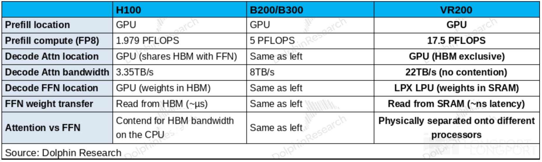
Across H100 -> B200/B300 -> VR200 NVL72: H100 to B200/B300 mainly increases raw compute with little structural change, helping Prefill. B200/300 to VR200 is a larger architectural shift that explicitly splits inference into three stages.
LPUs keep FFN weights in on-chip SRAM, but KV cache still sits in HBM. Single-access latency does not change; the gain comes from reduced transfers. That is the core latency benefit.
In sum, VR200 + LPU suits 'long context + high interactivity + large MoE' scenarios (e.g., DeepSeek-V4, Kimi K3), whereas the disaggregated setup is less optimal for 'short context + low interactivity + Dense' models (e.g., GPT-3 175B, Llama 70B).
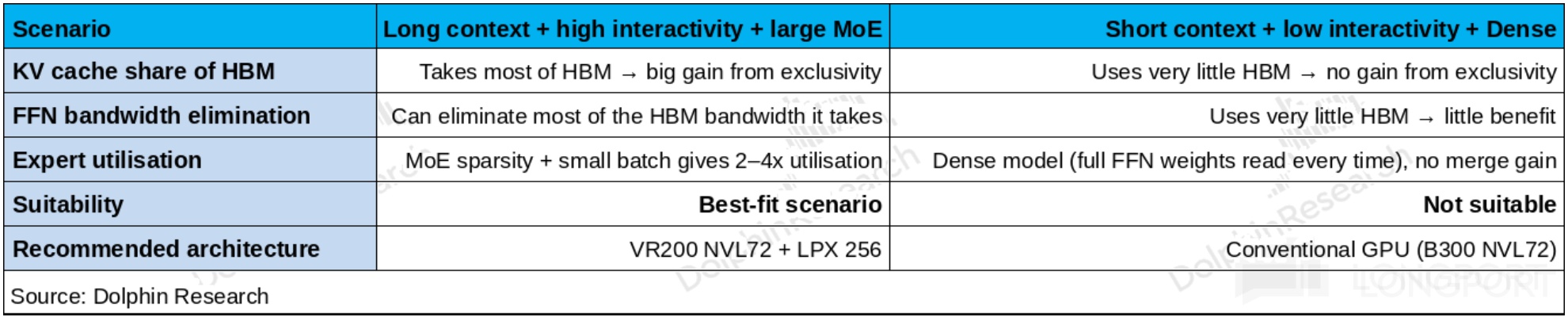
Note: short context = short dialogs (a few thousand tokens); very large hidden dimensions = very wide layers, with 32k+ models having FFN layers up to 11.3GB each. This drives memory needs.
III. How is Cerebras’ WSE built?
GPU vendors’ disaggregation and LPU adoption relieve HBM congestion to a degree. Since LPUs only hold weights, KV cache remains in HBM and is still constrained by 22TB/s HBM bandwidth.
By contrast, in the Cerebras WSE, KV cache also sits in on-chip SRAM with on-die bandwidth of 21PB/s, and read latency under 1ns (vs. 0.1–1µs on GPUs). This suits low-latency, speed-at-any-cost buyers.
WSE diverges from GPUs and therefore its manufacturing flow is very different. Cerebras’ wafer-scale chip is one of the most disruptive designs in semiconductor engineering. Rather than ‘dice-then-package’, WSE treats the largest square cut from a wafer as a single monolithic die.
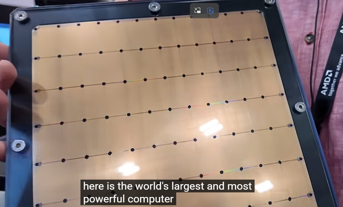
As shown, WSE cuts a 21.5cm x 21.5cm square from a 300mm wafer, with no internal dicing. It uses reticle stitching.
The die area is ~46,000mm², but lithography exposure has a reticle size limit — max single-shot area ~26mm x 33mm = ~858mm² (one reticle field).
The stepper must expose 84 times on the wafer to cover the square, matching the 84 WSE dies. That maps 1:1 to the tile grid.
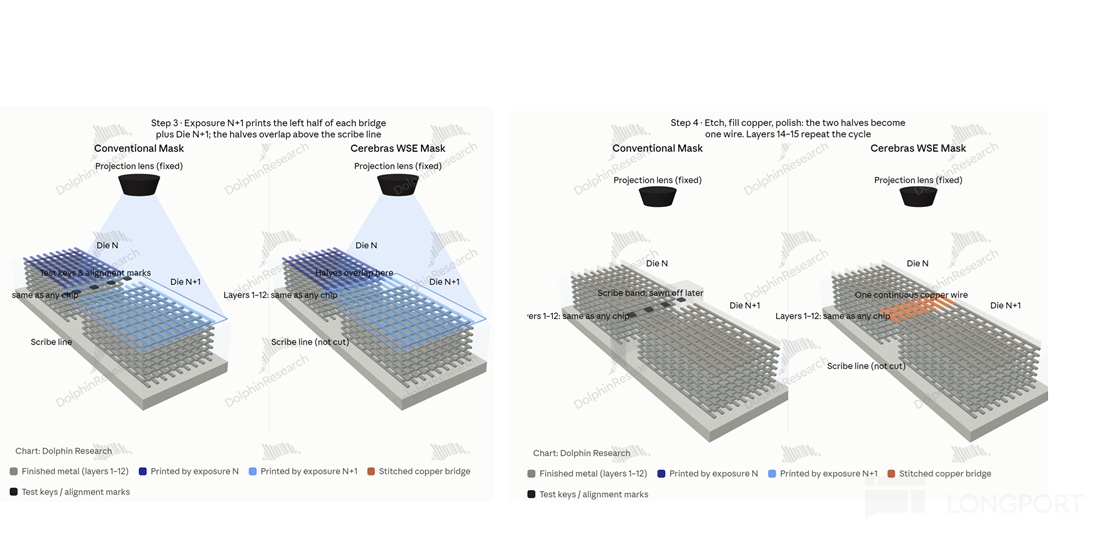
In the standard flow, these 84 exposure fields leave scribe lanes for dicing. WSE instead keeps the scribe lanes, but during top metal layers it uses special masks to draw micron-scale copper ‘bridges’ across the scribe lanes purely as physical links, stitching the 84 tiles into a high-BW 2D mesh. Those lines are what you see above.
Given how different WSE is, how does Cerebras actually manufacture it?
It runs through ‘wafer -> layout & routing -> FEOL (litho) -> mid-process test & fault tolerance -> packaging/assembly -> system integration’. The macro flow mirrors a normal chip, with key differences in several steps.
Step 1: Wafer manufacturing (standard)
WSE starts from standard 12-inch (300mm) high-purity silicon wafers, identical to any advanced chip. From refining quartz (SiO₂), purification, CZ pull, slicing, polishing, and cleaning, you get the wafer. No difference here.
Step 2: Layout design and routing (WSE-specific)
Conventional chips: the fabless designer uses EDA to tape out and hands masks to the foundry. WSE’s core micro-architecture is unique and is led by Cerebras.
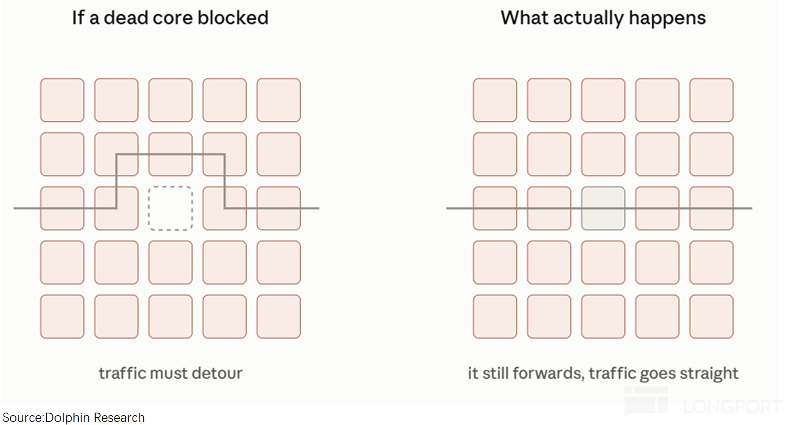
‘Layout & routing’ is not only physical geometry but also the compiler’s runtime logical placement — across 84 compute tiles, jobs must route around defective blocks, which underpins WSE’s fault tolerance. This is central to resilience.
This step involves:
i) Core micro-architecture: design a 38,000µm² core with 48KB SRAM (8 x 6KB banks, 32-bit per bank) + compute engine (SIMD ALU, 8 micro-thread contexts) + 5-port router. A custom ISA, neither ARM nor RISC-V.
ii) Tile replication within a reticle: replicate the core array across a reticle field. Reticle max ~858mm² (26mm x 33mm); each compute tile is ~550mm² hosting ~11,548 cores.
iii) Redundancy and reroute logic: bake spare cores, spare routes, and detours into the layout to survive block faults. This design-time cost does not vary with TSMC defect density.
iv) Scribe-lane routing design: short inter-die bridge patterns. This requires TSMC-provided scribe-lane design rules, which are outside standard PDK documentation.
v) Tapeout: use off-the-shelf EDA for synthesis, PnR, DRC/LVS. The only disclosed external IP is Synopsys DesignWare SLM for on-die sensing (distributed thermal, voltage, and process monitors across ~46,000mm²).
Step 3: FEOL (lithography — the WSE fork)
Following standard FEOL (clean -> oxid/diffuse -> deposition -> litho -> implant -> CMP -> metallization), WSE runs the same steps, using step-and-repeat to expose the same mask 84 times (~550mm² per tile).
Note: step-and-repeat projects the mask pattern (reduced) to one field, then moves the stage and repeats. WSE3 uses TSMC N5, typically ~15 metal layers.
Each metal layer runs the same four-step loop: i) deposit dielectric (full wafer); ii) litho pattern (84 steps); iii) etch trenches/vias (full wafer); iv) Cu fill + CMP (full wafer). Repeat ~15 times to build the stack.
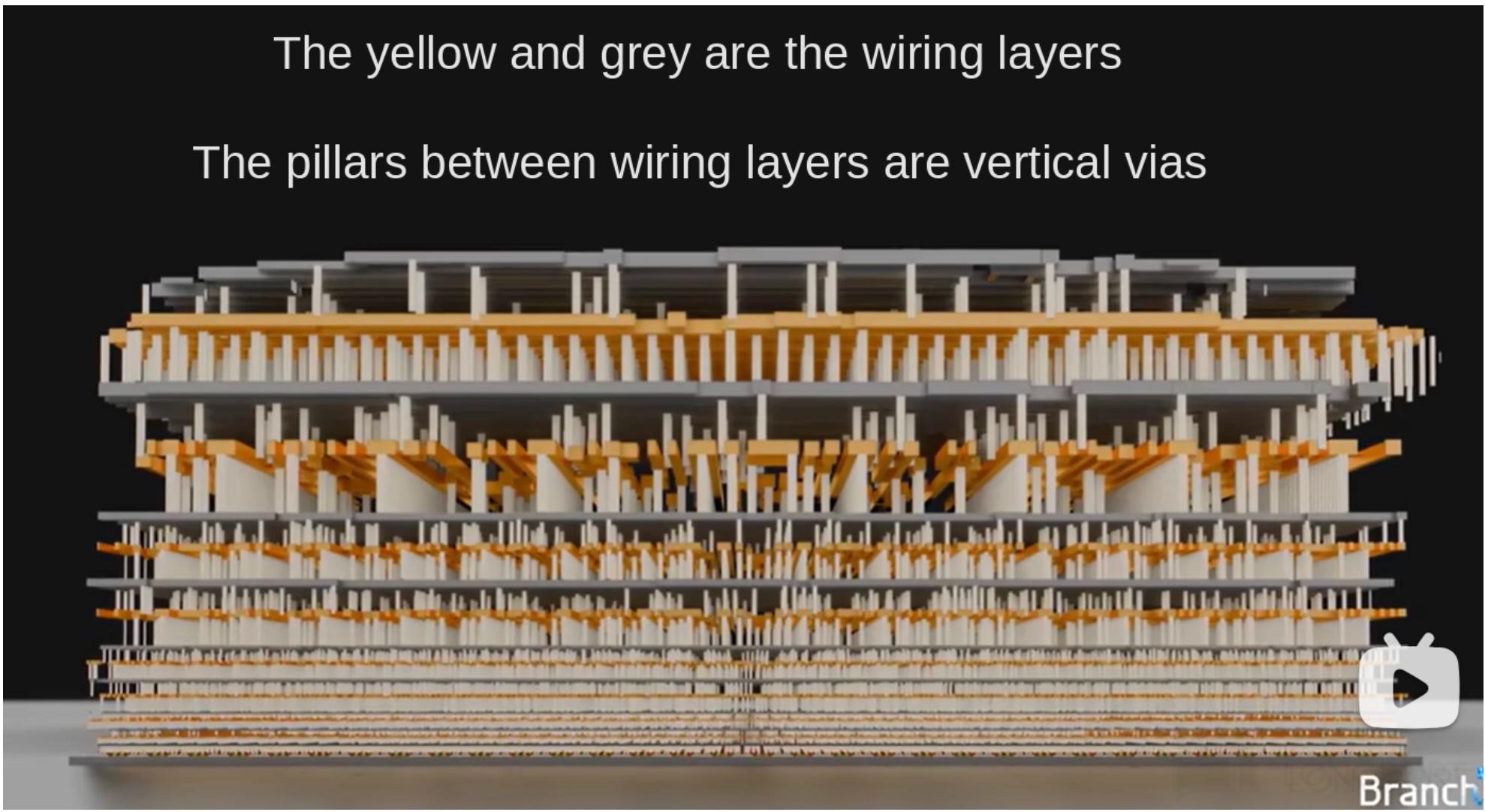
In practice the first ~12 layers are similar; the divergence appears at layer 13 and above where WSE’s masks change.
On conventional masks, the scribe lane holds process monitors, alignment marks, and test keys. It is destined to be sawed off, so geometry there is inconsequential.
On Cerebras’ masks, that lane becomes a routing channel. Short metal bridges cross die boundaries, under 1mm long, using wafer-scale interconnect across scribe lanes — effectively skybridges on the top floors.
This is the key: one bridge is split across two exposures — half drawn at the right edge of field N, half at the left edge of field N+1. Field N (tile body + right half-bridge) -> step -> field N+1 (left half-bridge + tile body) -> the two halves meet over the scribe to form a complete wire.
Because the bridges span fields, masks must change. No extra exposure steps are added; alignment relies on stepper precision. Process steps mirror the earlier layers, with masks carrying the bridge features.
The copper over scribe lanes and inside dies is deposited, etched, and planarized in the same runs, using the same tools, materials, and parameters. There is no out-of-flow step.
Why top layers? Lower layers are too fine; nm-scale misalignments would open or short wires and kill yield. Upper layers have µm-scale tolerance, two to three orders more forgiving.
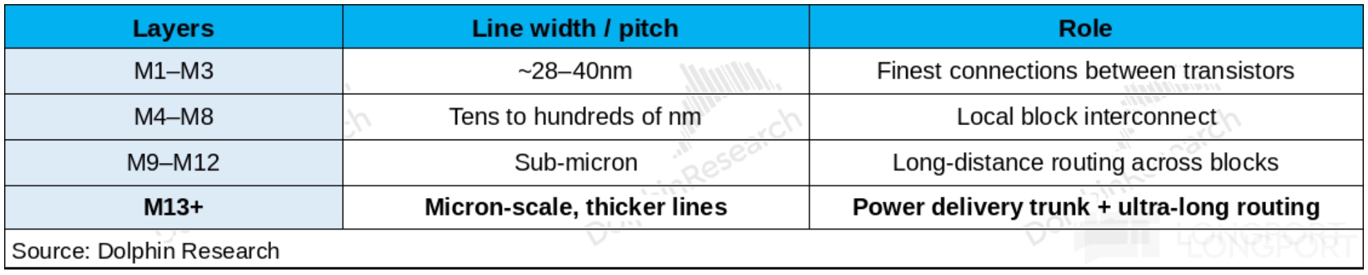
One top-layer bridge is theoretically sufficient, but for routing flexibility and redundancy they likely use 2–3 layers. Scribe lanes are a dicing ‘no-go’ region on normal wafers; Cerebras routes over them to tie all 84 tiles into one fabric.
Step 4: Mid-process test & fault tolerance
Traditionally, before dicing, each die is electrically tested; bad dies get inked or mapped. After sawing along scribe lanes, bad dies are discarded and good dies go package.
For WSE, the goal is not to select good dies, but to locate which cores on the wafer are faulty and where. The 84 tiles are stitched into one, with I/O only at the perimeter. There is no physical access into the interior, so WSE uses full-wafer self-test.
Each core has local SRAM (48KB) and a router, so each can run self-test and report results over the mesh — the minimal hardware needed for core-level BIST. Results classify failures:
i) Router failure: the local path is down; the tile cannot report and traffic cannot transit, creating a blacked-out region. You must distinguish tile failure from path failure.
They probe via redundant routes (e.g., from multiple directions/edge ports) to diagnose. Hence cores were designed with N/E/S/W redundant paths.
ii) ‘Bad core’ classification: Core = compute + local SRAM + router; compute/memory and routing are physically separate. If the router is alive but compute/memory is bad, the core can still act as a forwarder. If the router is dead, the core is considered hard-dead regardless of compute/SRAM health.
Step 5: Packaging/assembly
For WSE, TSMC handles FEOL wafer build and in-fab wafer-scale interconnect. Packaging and system assembly are handled by Cerebras ex-fab.
After FEOL, before delivery TSMC completes cross-scribe metal interconnect (co-developed) and full-wafer passivation and bumping (passivates the intact 300mm wafer and adds dense micro-bumps/C4 bumps to fan out power and signals).
In short, TSMC ships a 300mm wafer with micro-bumps and cross-reticle interconnects. The subsequent system-level packaging is not done by TSMC and is fully developed by Cerebras.
This is a 300mm wafer, 775µm thick, with no power pins, no data ports, and no cooling. Cerebras’ job is to turn this wafer into a machine.
They first trim the 300mm circle to a 215mm x 215mm square, discarding the crescent edges (about 35% area waste) to get the final square die. That yields the form factor.
Next come two hard problems: I/O and power delivery. The footprint is huge, and peak power is 23kW (like a dozen home induction hobs at full power). Conventional packaging would self-immolate on power-up.
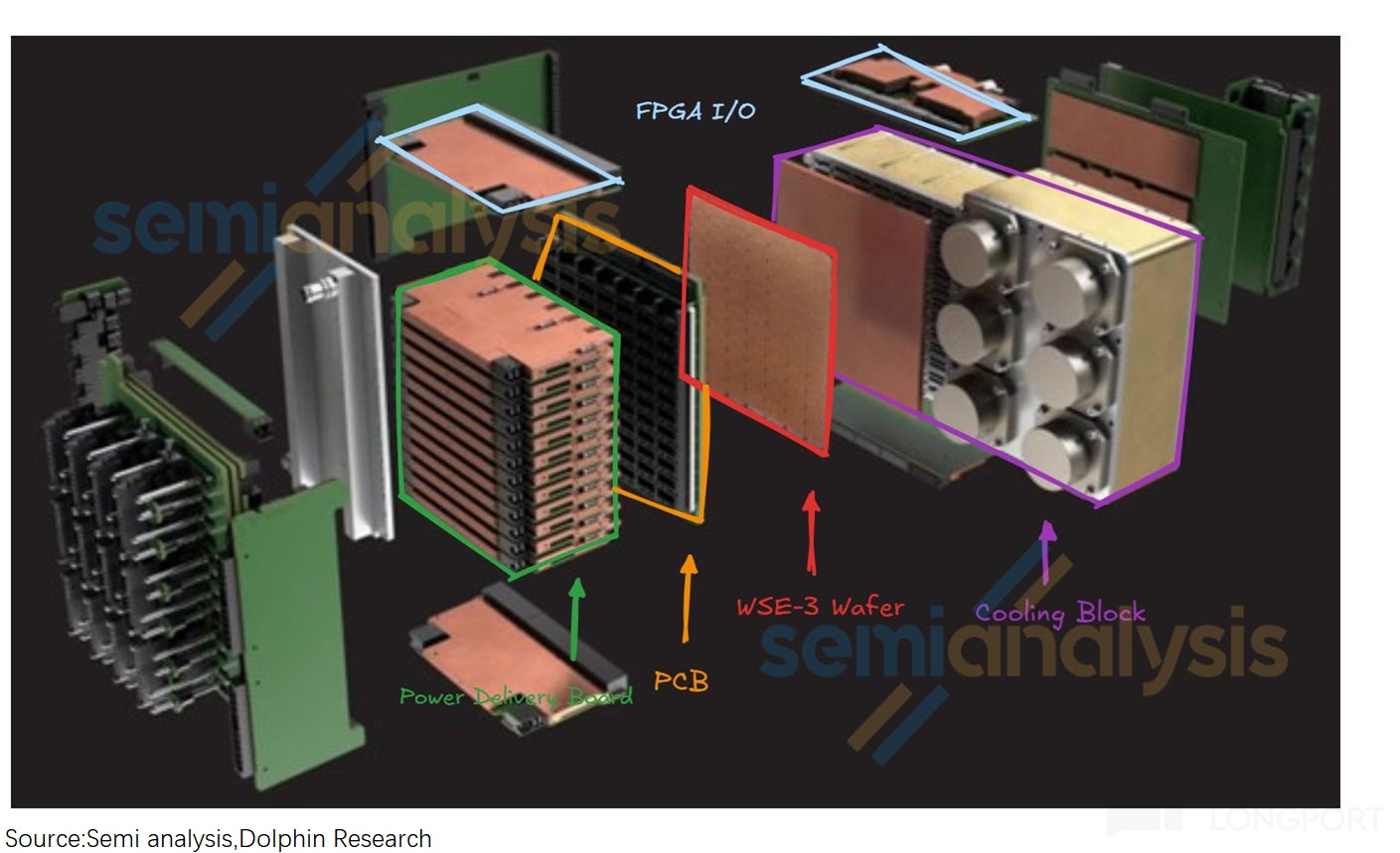
Cerebras designed a four-layer ‘sandwich’ — cold plate + wafer + elastic interposer + PCB — called the ‘engine block’. This is the company’s core packaging innovation.
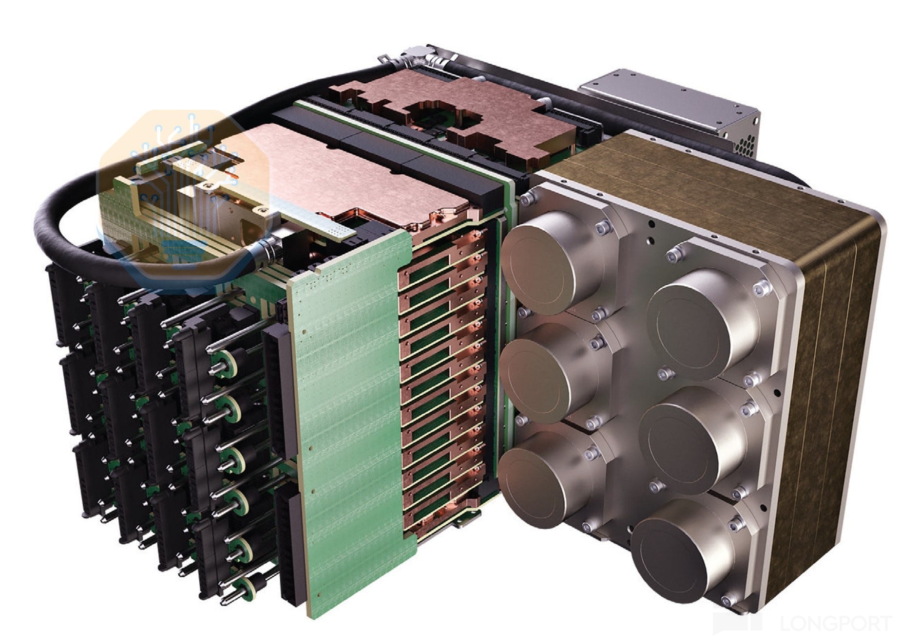
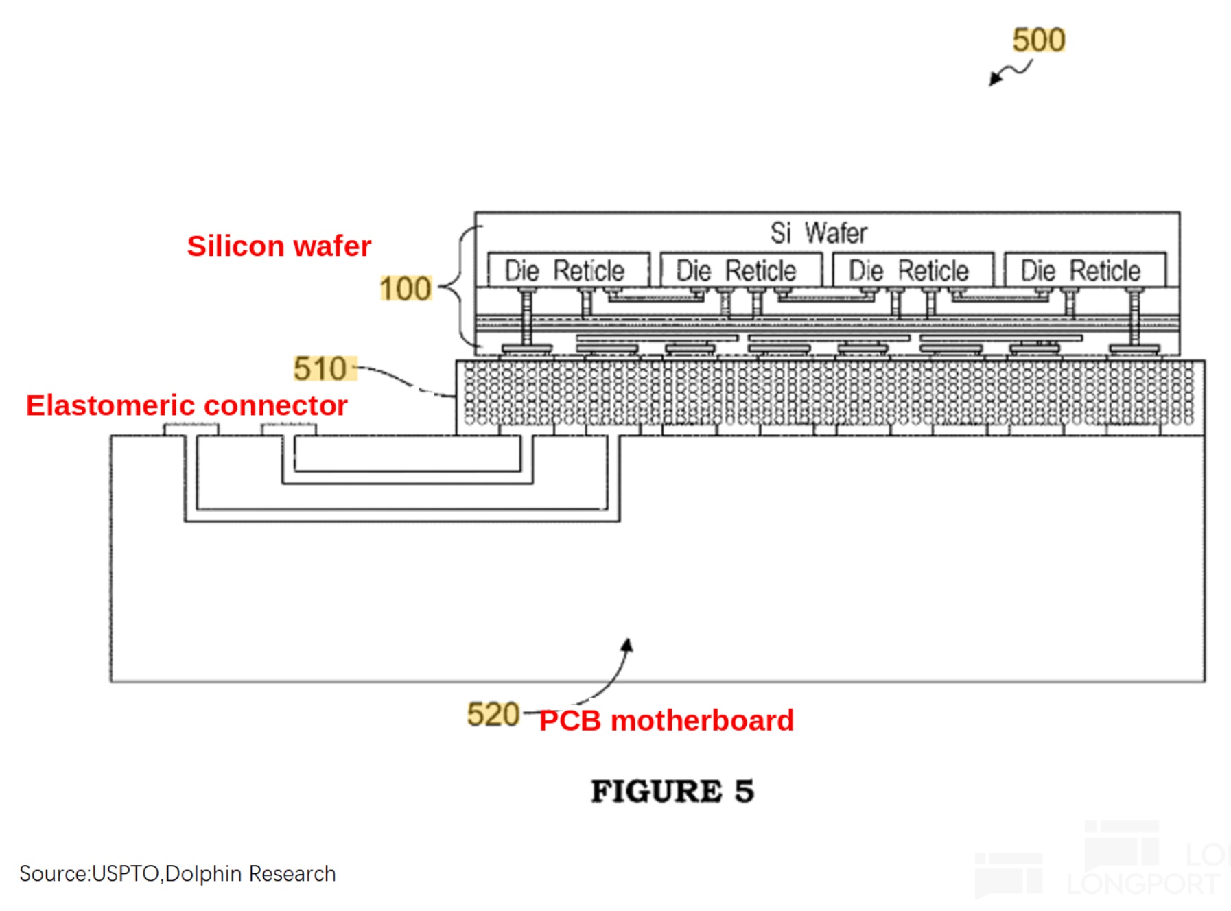
i) First, mount the 215mm-square wafer to a PCB — solder is not viable as thermal cycling would tear joints. Silicon and FR4/Cu expand at very different rates, so solder balls would shear off once the die heats.
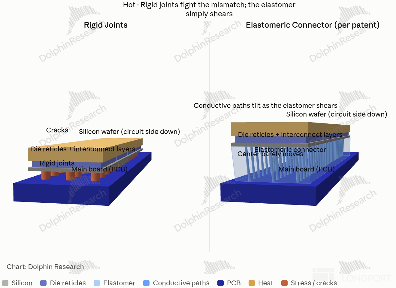
Cerebras uses a custom elastic connector with micro-springs/flexible contacts between wafer and PCB — a gasket of millions of micro-springs absorbing the CTE mismatch.
As the die heats and expands, springs flex laterally; as it cools, they recover. This ‘soft compliance’ dissipates destructive thermal stress.
ii) After electrical attach, implement 3D vertical power delivery.
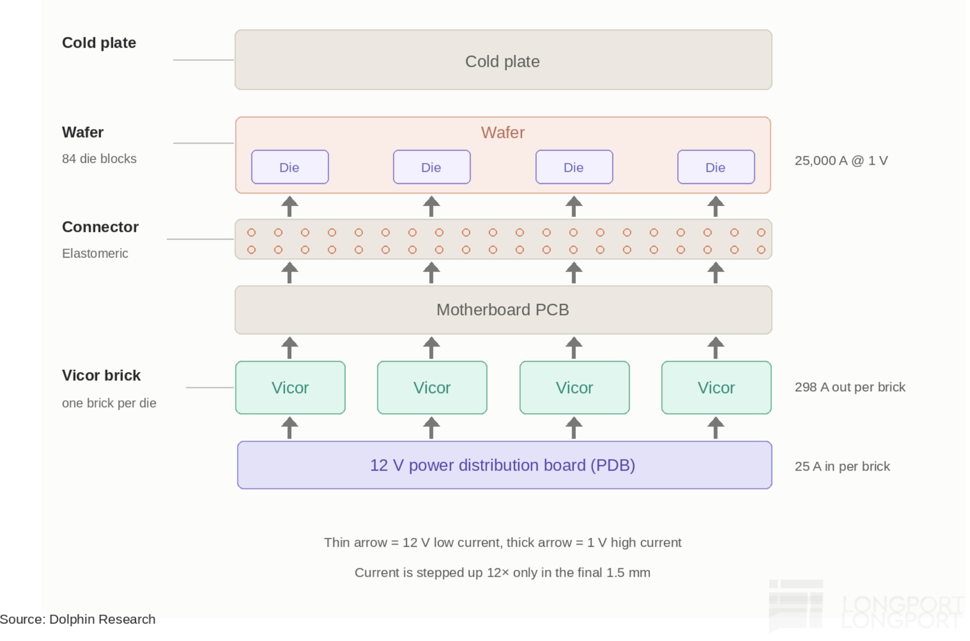
WSE peaks at ~23kW, while core voltages are ~0.8V, implying currents over 20kA — enough to melt steel cables. Edge feeding fails because a) the distance to center is ~10cm, with severe IR drop, starving the center of voltage.
Cerebras places the VRM directly under the wafer, feeding vertically up to the backside. It inputs 48V (even 54V) to keep currents lower and thermals manageable, then point-of-load steps down to ~0.8V and distributes to all 84 tiles. This shortens paths and curbs losses.
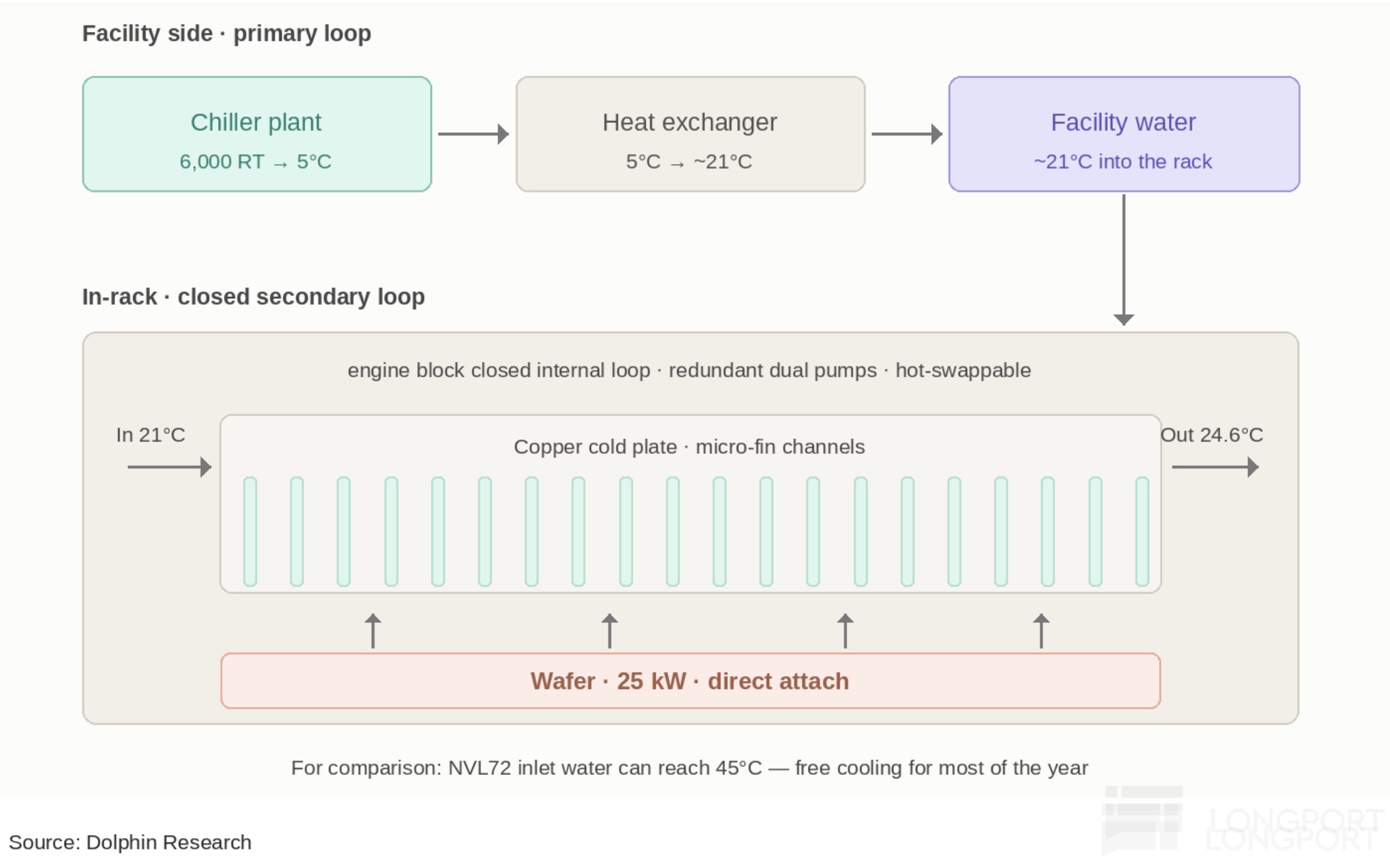
iii) Finally, attach a direct-contact micro-channel water-cooling cold plate for this 23kW ‘furnace’.
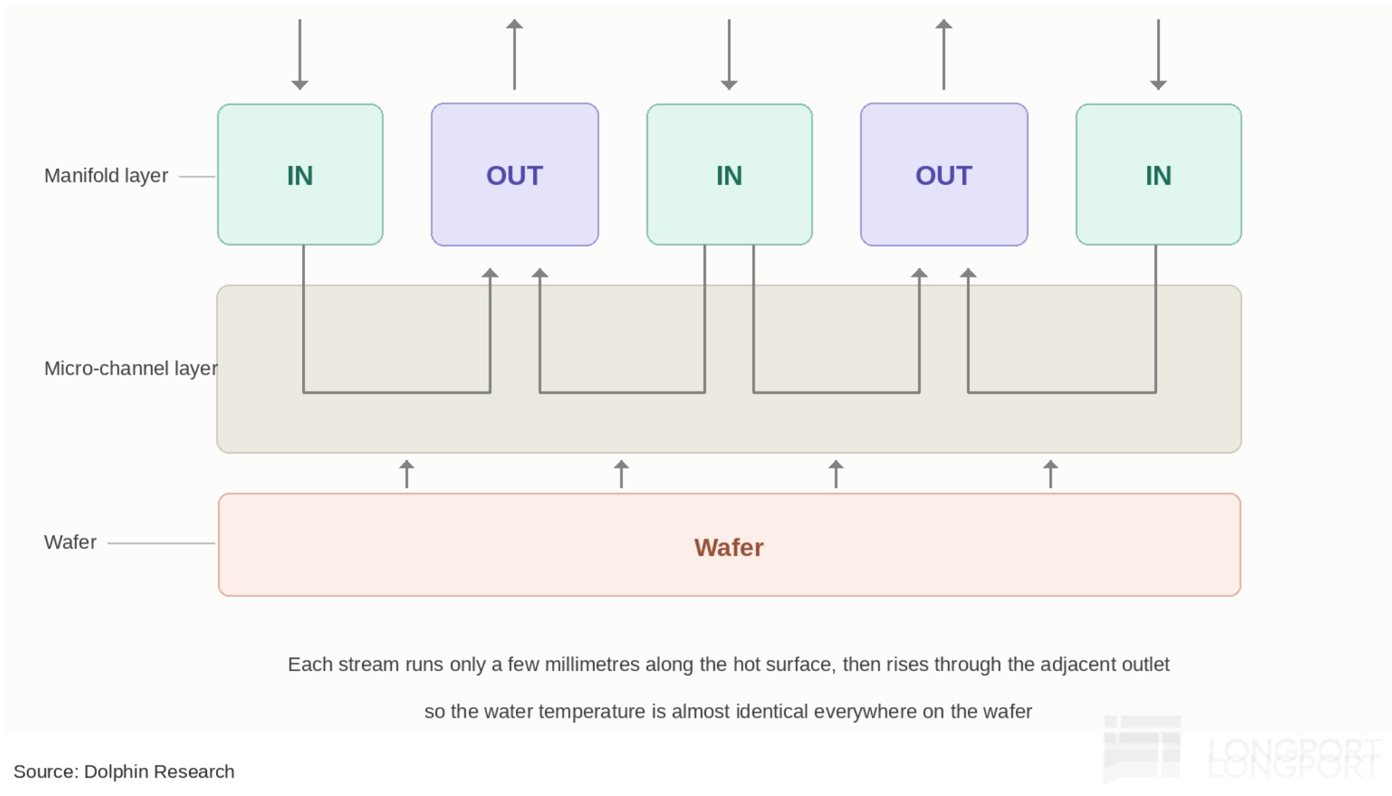
The cold plate is copper with micro-fins on the back and a polished face pressed against the wafer; coolant flows through the channels to remove 20kW+ of heat. Interface design uses polished sliding contact + preload + relative slip to reduce thermal resistance and avoid shear.
Cerebras abandons conventional single-pass flow and implements a vertical 3D manifold. The cold plate is partitioned into hundreds or thousands of micro cooling cells; coolant from a top manifold jets vertically into local regions like an array of tiny showers.
With i) + ii) + iii), the four layers (cold plate + wafer + elastic connector + PCB) form the engine block, with all electrical (wafer-to-PCB) and thermal (wafer-to-cold plate) interfaces held by pressure.
Given the 215mm x 215mm x 775µm, 83g bare silicon, uniform pressure is critical; total clamping force can reach 4 tons or more. After compression, fixtures lock the wafer between PCB and heat exchanger to maintain force over time.
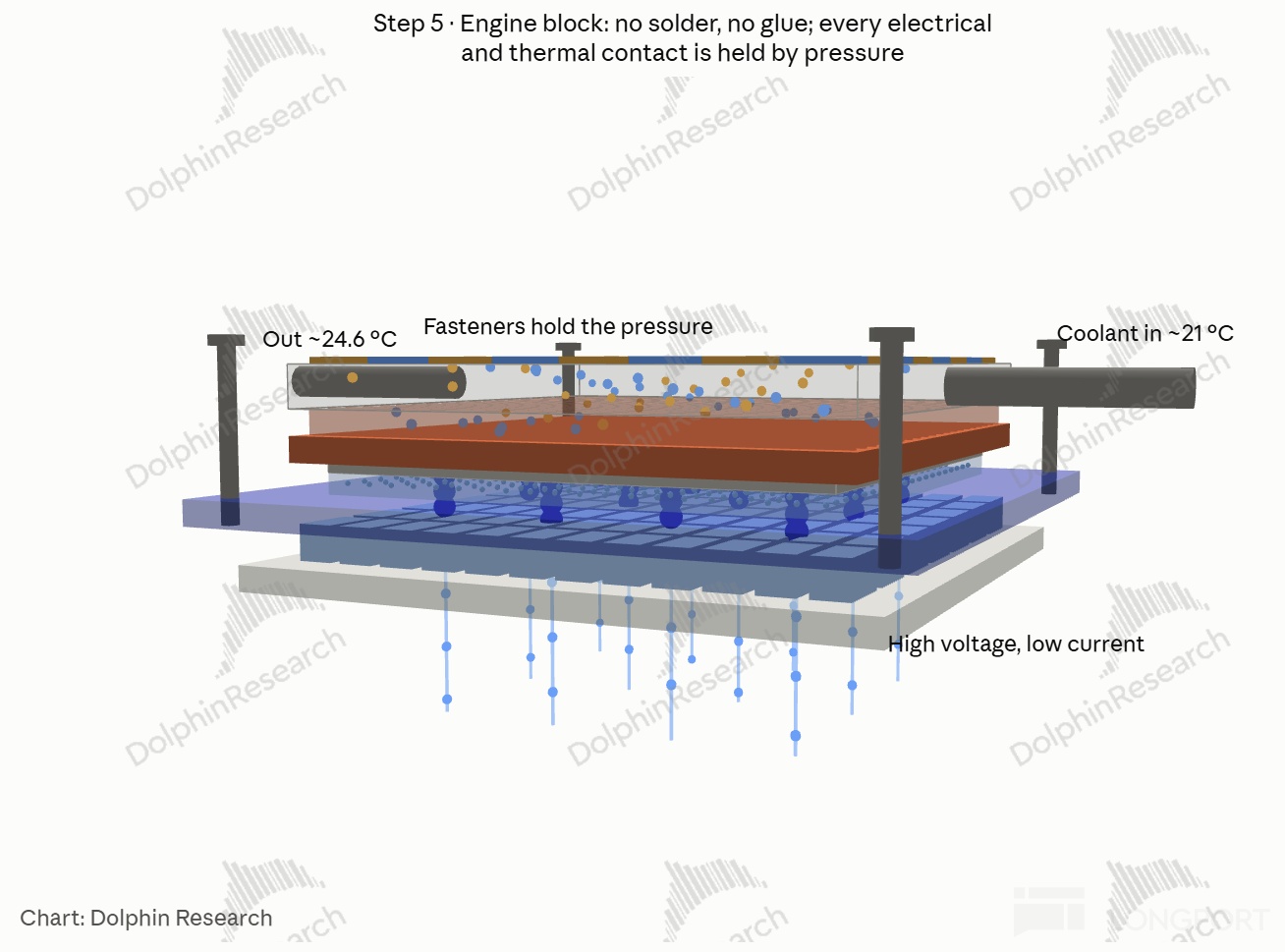
Any local pressure hot-spot will crack the die, so it is not just ‘apply 4 tons’, but distribute it extremely evenly over ~0.5 sq ft. The assembly machinery is therefore fully custom.
From four-layer stack to WSE module is a two-step ‘insert + press’ process: plug the wafer into the PCB via elastic sockets, then press the polished cold plate against the back under preload. Cerebras’ in-house tooling performs the lamination, then connects the fluid manifold to complete the module.
Step 6: System integration
From engine block to a full compute system, you add I/O receivers, power, liquid cooling, and heat rejection. All integration and testing are done in-house by Cerebras.
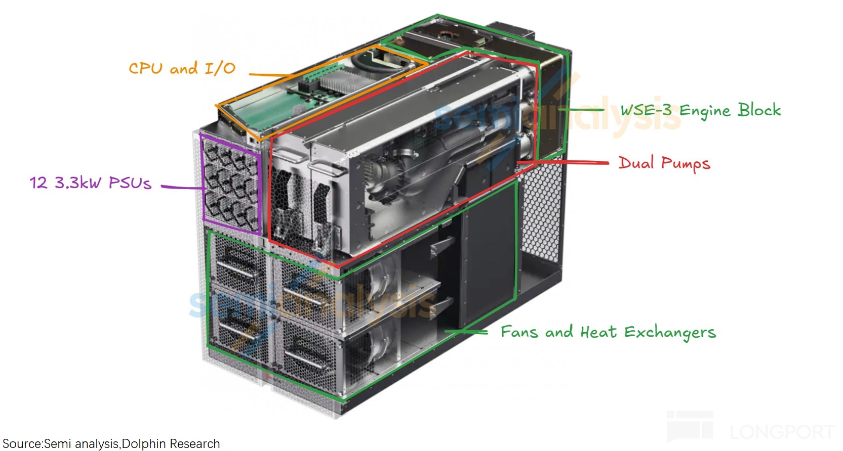
i) I/O receiver: mount an I/O FPGA module (NIC-like) on top of the engine, connected to the WSE PCB via board-to-board connectors. It carries Cerebras’ proprietary I/O and converts it to Ethernet for scale-out and PCIe for host connectivity.
ii) Power and liquid: a) 12 x 3.3kW PSUs + 12 PDBs blind-mate into the engine block; b) connect the cold plate to chassis brass manifolds, and install dual pumps (one redundant), the heart of the cooling loop.
iii) Heat rejection: coolant circulates inside the rack, but heat must be expelled outdoors. The cold plate’s heat must be handed off via a heat exchanger to facility chilled water or outdoor air.
These six steps comprise the full CS system build. Steps 2–6 are largely owned by Cerebras, notably the complex layout/routing, mid-process test/fault-tolerance, and advanced packaging/assembly; TSMC mainly contributes FEOL lithography.
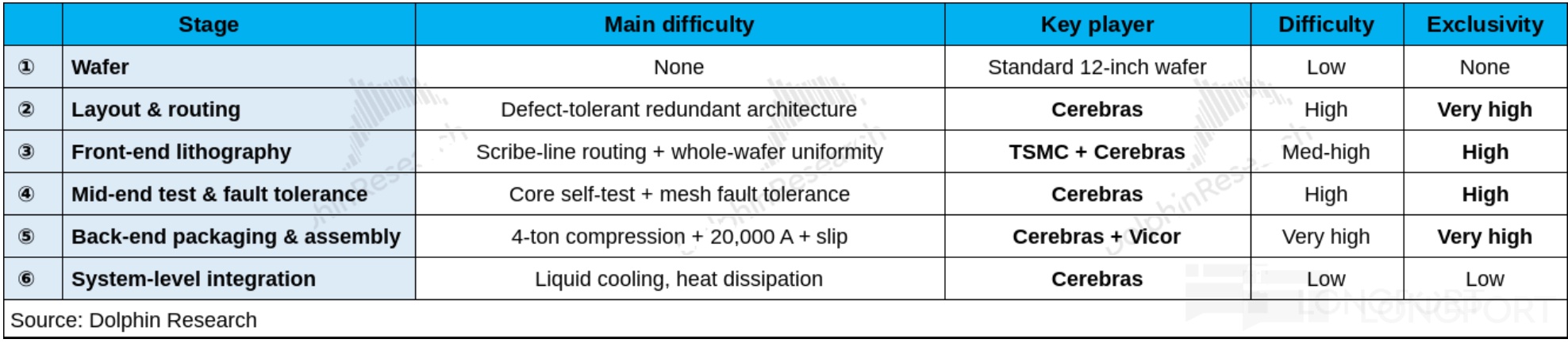
Rack-level assembly and test are internal, and the deliverable is a turnkey rack. Note that a Cerebras system is not plug-and-play on arrival; it needs site readiness:
Facility assessment -> data hall retrofit -> rack install and hookups (water, power, fiber) -> external systems (host servers, Memory X [4TB–2.4PB weights], SwarmX [multi-system broadcast & collectives]) -> software stack & model load (CSL, Cerebras compiler) -> ongoing ops.
This makes CS’ facility retrofit costly, but its target customers are those who can turn milliseconds into revenue (OpenAI, AWS, HFT, real-time interactivity). For such use cases, the WSE’s 21PB/s on-die BW delivers speed GPUs cannot match.
This article unpacked what WSE is, which GPU bottlenecks it addresses, and how it is manufactured and where it is hard. The next piece will cover Cerebras’ biz. performance and outlook — stay tuned.
<End>
Risk disclosure and statement: Dolphin Research Disclaimer and General Disclosure


The copyright of this article belongs to the original author/organization.
The views expressed herein are solely those of the author and do not reflect the stance of the platform. The content is intended for investment reference purposes only and shall not be considered as investment advice. Please contact us if you have any questions or suggestions regarding the content services provided by the platform.