

CXMT 4F^2: Will it disrupt the memory triopoly?
 I'm LongbridgeAI, I can summarize articles.
In the first part (see link), Dolphin Research started from 1T1C, explaining why 6F² planar transistors stalled scaling. It also showed how VSG vertical surrounding-gate stacks the capacitor, bitline, and wordline, shrinking cell area from 6F² to 4F² to pack nearly 50% more cells at the same node.
But being able to build it is not the same as building it well. Where is 4F² hard, when will Samsung, SK Hynix, and Micron adopt it, and what would CXMT’s year-end first-gen launch mean for DRAM pricing and Big 3 margins. The answers follow.
Detailed analysis follows:
I. Where 4F² is hard, and what it changes
1.1 Not CXMT-only: industry consensus and Big 3 timelines
First, 4F² is not CXMT’s proprietary invention. Vertical-channel transistor research has been ongoing for years, and earlier efforts were shelved mainly because arrays and periphery shared one process flow, making a 6F²-to-4F² architecture change uneconomic.
As 6F² scaling gets tougher and hybrid bonding matures, 4F² has re-emerged as the next-gen consensus. Industry checks indicate all three majors are evaluating it, and some have pulled forward their plans. By company cadence:
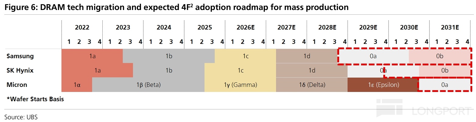
Samsung: fastest so far, but with route wavering. Per The Bell (Aug), Samsung originally aimed to finish 1d development in Sep, shift to production in Dec, and begin initial volume around end-2027. The next 0a node (Samsung’s 10a) was slated to move to 4F².
Per The Elec (Apr), Samsung produced wafers on 10a in Mar and confirmed working chips in tests, targeting development completion within the year, qualification in 2027, and volume ramp in 2028. The following 10b and 10c nodes would retain this structure. On current read, Samsung appears ahead in 4F² R&D and know-how.
SK Hynix: likely one node later. Hynix still prefers to keep 6F² at 0a. The Elec (Apr) reported Hynix plans to introduce 4F² and vertical transistors at 0b, one node behind Samsung.
From recent node progress, The Bell (Aug) noted Hynix plans to complete 1d development in Dec, while Samsung planned Sep. That gap already shows in this generation.
At 1d, Hynix is about three months behind in development completion and around half a year behind in mass-production readiness. Naturally, migration to the newer 4F² architecture should be slower as well.
Micron: path unclear, likely latest. Micron has not publicly disclosed a 4F² plan, and external takes differ: some Korean media in 2025 suggested Micron may skip 4F² and go straight to 3D DRAM. UBS (Jan) now believes 4F² is back on its roadmap, with 0a pivoting to 4F² and H2 2030 as the mass-production window.
CXMT: first-gen announced; mass scale to be validated. Since inception, CXMT has pursued 4F², and per its president, the first-gen 4F² will target DDR5 RDIMM and is expected by year-end. Timing-wise, that is earlier than the Big 3’s nodes (Samsung’s plan was to ramp in 2028).
However, the wording was launch rather than mass production. With no disclosed specs, yields, or shipment scale, year-end is more likely a release, sampling, or small-batch validation.
1.2 Where 4F² gets hard
Where are the difficulties. They boil down to the following.
First, the floating-body effect. With the bitline buried at the base, the silicon pillar is isolated from the substrate, leaving the mid-pillar p-type region electrically floating and prone to charge accumulation. That drives Vt drift and can cause data loss or errors. The industry is exploring mitigations such as adding a back gate.
Second, the process sequence of ‘bitline first, then grow pillars’ is nontrivial. In the new stack, the bitline sits below the pillars, yet the pillars need high-quality single-crystal silicon. One route is to grow the pillars epitaxially above the bitline, but epi capacity and uniformity are challenging.
Another is a backside flow: build pillars on the front side, flip the wafer and thin from the back, then form the bitline at the pillar base, typically requiring special wafers such as SOI. This adds more steps and complexity.
A third route is to form pillars and bitlines on separate wafers and connect them via wafer-to-wafer hybrid bonding, directly joining copper pads face-to-face. This has volume precedent in 3D NAND, such as YMTC’s Xtacking.
Third, process decoupling between array and periphery. Vertical-transistor arrays and periphery logic have very different process requirements, and co-fabrication on one wafer constrains both, which stalled early 4F² attempts. CXMT’s disclosed path fabricates them separately and integrates via wafer-level hybrid bonding, raising demands on bonding yield, alignment, and cost.
Fourth, materials and resistance. With only about a 1F gap between adjacent pillar rows, both pillars’ gate oxides, their surrounding wordlines, and the inter-wordline dielectrics must all fit into that slit, leaving very little space for the wordline metal; bitlines face similar constraints. Thinner lines mean higher resistance, slower signal propagation, and degraded memory performance, so the industry is evaluating Mo and Ru for wordlines (gates) instead of TiN/W, as they suffer less resistivity rise at extreme widths.
Fifth, tighter coupling and yield ramp. Denser pillars and wordlines increase coupling between adjacent lines, and 6F²-era designs and flows are not directly reusable. A new integrated flow is needed, and first-gen yield ramp will take time.
All in, CXMT’s announcement suggests 4F² has moved from ‘whether to do it’ to ‘can be done’. When it can scale to volume and with what quality is a separate question.
II. Implications for DRAM and the Big 3
Back to the opening question: how big is the impact on DRAM and the Big 3. Dolphin sees it differently in the near term vs. the medium to long term.
Near term (2026–2027): limited direct S/D impact. CXMT has only pre-announced a first-gen part with unknown specs, yields, and scale, and new architectures usually need lengthy ramps to become capacity drivers. Given Big 3 timelines, meaningful 4F² output likely arrives only from late 2028, implying little change to the current S/D view through 2028. Recent share weakness for the Big 3 reflects concerns about CXMT’s catch-up pace rather than immediate fundamentals.
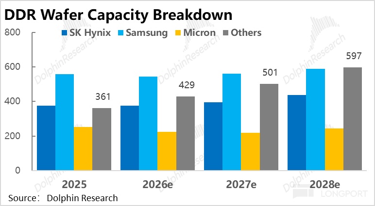
Medium/long term (post-2028): upside risk to supply growth. 4F² effectively pulls forward roughly two nodes of density in one step, lifting bit output per wafer by about 30–50%. Dolphin estimates that roughly 75% of incremental DDR wafer capacity in 2026–2028 already comes from domestic players, before any 4F² per-wafer uplift.
If CXMT truly starts 4F² DDR volume in 2027, supply could exceed prior expectations. Without sufficient demand, the S/D balance could flip and DRAM pricing could fall meaningfully.
While CXMT has not cracked HBM, DDR and HBM currently carry near-par GB pricing, with DDR at lower manufacturing cost, making DDR the main profit pool. By Dolphin’s prior estimates, over 70% of SK Hynix’s DRAM GP in 2028 would come from conventional DDR.
Hence, if CXMT’s 4F² yields and capacity ramp well, the profit hit to the Big 3 could be significant. The risk is non-trivial.
By player:
CXMT: the biggest win is a non-EUV catch-up path. As 6F² scaling advances, it leans more on EUV, which CXMT cannot procure under export controls, forcing DUV multi-patterning with rising cost and yield pressure. 4F² trades architecture for density and relaxes design rules, giving CXMT a chance to approach peers’ density under DUV-only conditions.
Combined with CXMT’s ongoing capacity adds and a first-gen entry directly into server DDR5, a higher-barrier and higher-margin segment within conventional DRAM, competitive pressure in conventional DRAM could intensify. That could reshape pricing power at the margin.
Samsung: a chance to claw back. Recent DRAM yield issues have also hampered its HBM progress, but Samsung appears ahead in node advances and 4F² technology. This could open a lane to overtake on newer-architecture products.
SK Hynix: little near-term change; mid-term depends on Samsung’s turnaround. Hynix is a node behind on 4F², but its current edge rests on HBM products and customers, which 4F² timing does not quickly alter. If Samsung uses 4F² to fix DRAM and HBM execution, Hynix’s HBM lead could narrow.
Micron: relatively passive. Micron had focused more on 3D DRAM, leaving it behind Samsung and Hynix on 4F², and UBS sees H2 2030 for volume. If Samsung and CXMT execute first on 4F², Micron could face a window of relative cost and density disadvantage.
Upstream suppliers: 4F² adds many steps, including selective epi, ALD, RTA, high-aspect-ratio etch, and hybrid bonding, with potential beneficiaries including Applied Materials, Tokyo Electron, Lam Research, ASM Intl, and Eugene Tech, while materials plays include suppliers of Mo and Ru (e.g., Merck). Lithography demand may be diluted in the first 4F² generation, but subsequent node shrinks still rely on tighter geometries and leading-edge litho.
<End of text>
Risk disclosure and statement:Dolphin Research disclaimer and general disclosure


The copyright of this article belongs to the original author/organization.
The views expressed herein are solely those of the author and do not reflect the stance of the platform. The content is intended for investment reference purposes only and shall not be considered as investment advice. Please contact us if you have any questions or suggestions regarding the content services provided by the platform.