

NVDA
212.1700.57%
D
10 hours ago
AMD vs. NVDA: Can Helios Measure Up?
 I'm LongbridgeAI, I can summarize articles.
The merchant GPU market for external sales is now essentially a duopoly between $NVIDIA(NVDA.US) and $AMD(AMD.US). AMD largely missed the AI compute boom in the MI300 era due to the lack of a system-level solution, namely an interconnect architecture. With Helios arriving, the questions are:
1) Has AMD truly gained the capability to go toe-to-toe with NVIDIA?
2) In the race and iteration of interconnect schemes, what shifts are occurring across the value chain, and who benefits or loses?
We approach the topic from the interconnect angle. For AI interconnect basics, cf. the previous primer.
Main text:
We start by comparing the interconnect differences between NVIDIA and AMD.
I. Soft power: ecosystem positioning
1.1 Scale-Up: NVIDIA’s gold standard vs. a coalition counterweight
NVIDIA: a closed ecosystem as the gold standard. NVLink is tightly integrated with the CUDA and NCCL software stack, delivering top-tier latency and bandwidth, but at a premium price. Its closed ecosystem effectively locks customers into NVIDIA’s stack. To ease concerns, NVIDIA will launch NVLink Fusion in 2025, partially opening NVLink to third-party CPU/xPU domains and turning it into a semi-open standard, allowing non-NVIDIA chips to attach to its chip domain.
AMD: banding together against NVIDIA. UALink is a coalition led by AMD to rival NVLink’s Scale-Up protocol, built around Infinity Fabric. AMD plans to open-source IF, add flexible I/O channels to support multiple standards, and drive the next-gen open standard UALink. Members include AMD, ALAB, AWS, Google, and Meta.
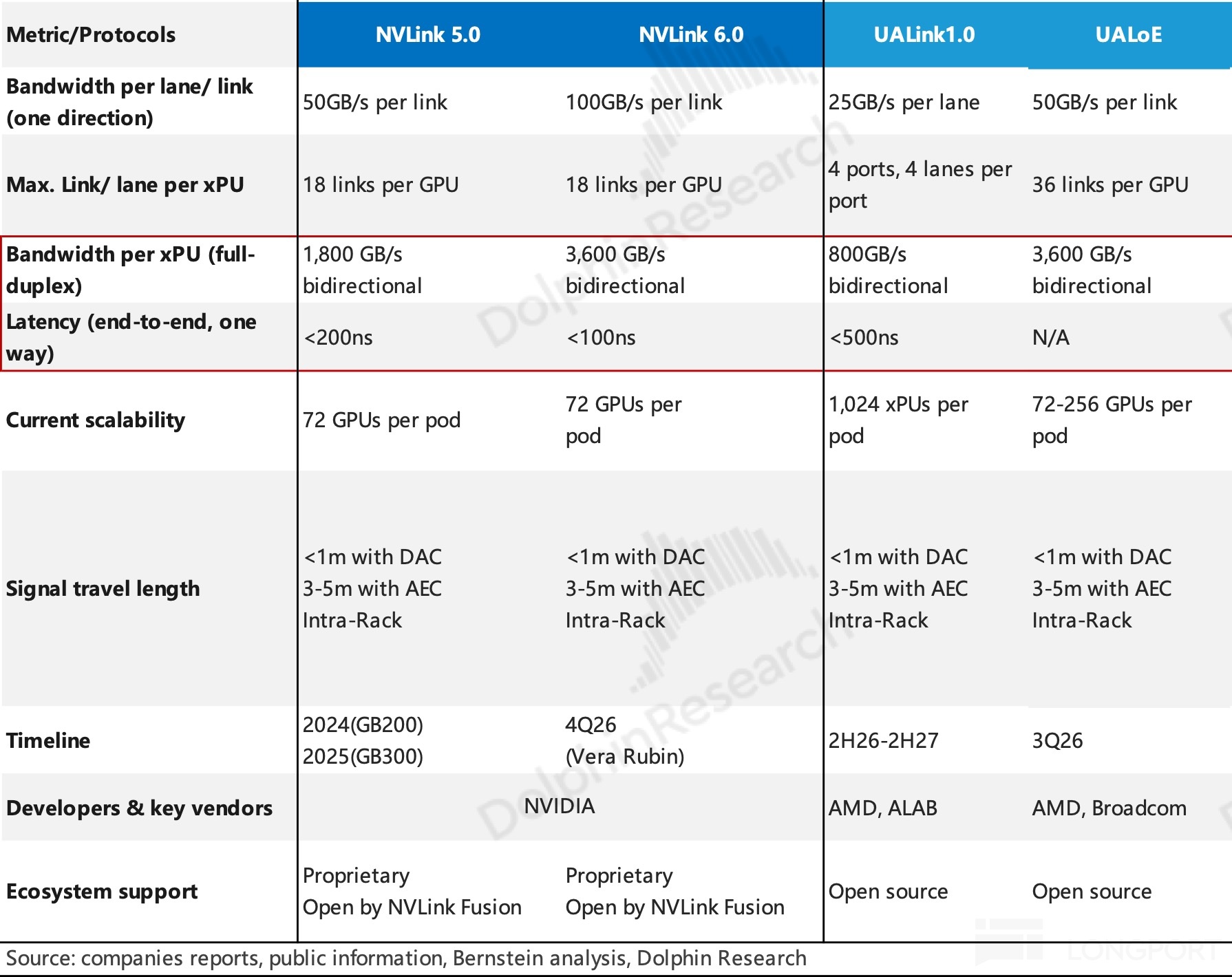
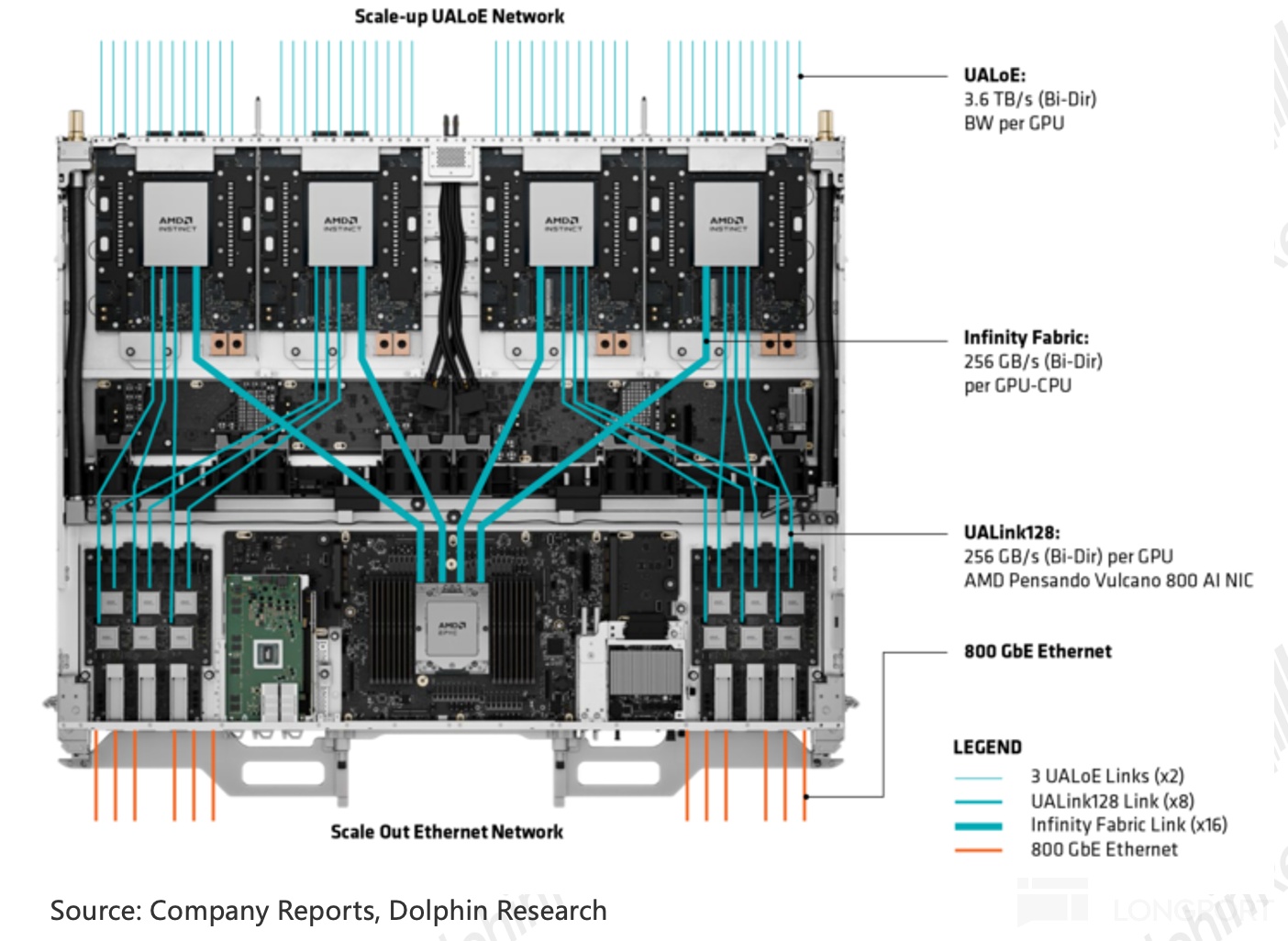
Loud alliance, thin hardware is awkward. Native UALink switch silicon is still under R&D and ramp at ALAB and Marvell, so Helios’ Scale-Up protocol currently runs UALoE (UALink over Ethernet) as a bridge. As shown below, UALoE bandwidth matches NVLink 6. Latency is undisclosed, but it likely trails NVLink because UALoE rides Ethernet, requiring repeated encapsulation/decapsulation between two stacks, plus Ethernet forwarding overhead.
1.2 Scale-Out: IB is costly and closed, Ethernet leads
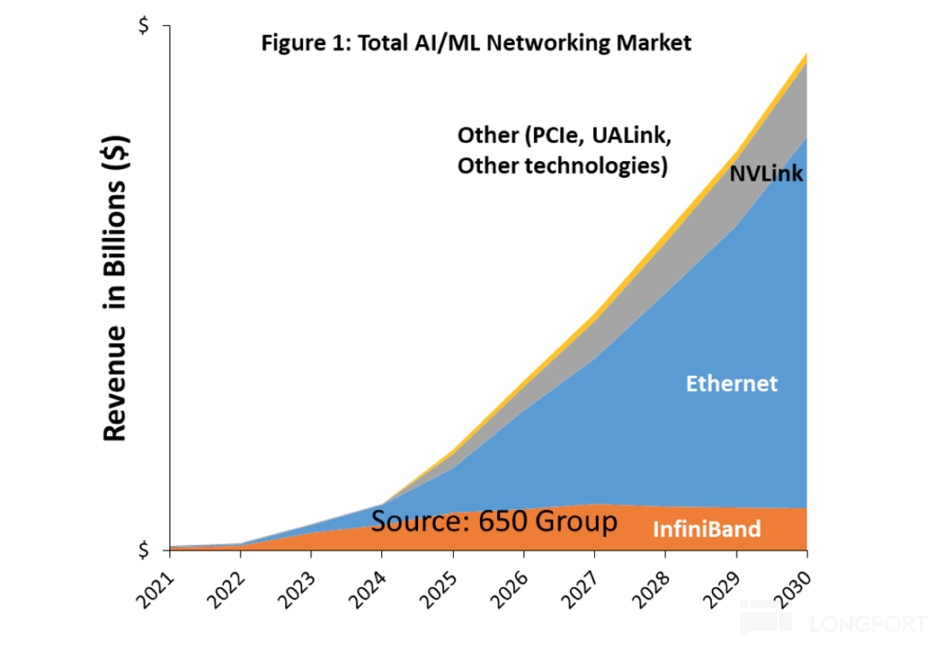
The Scale-Out landscape is clearer, with competition between NVIDIA-led InfiniBand and the open Ethernet ecosystem. NVIDIA’s core hardware includes Quantum switches, ConnectX NICs, and BlueField DPUs. The market has decisively tilted toward Ethernet. It offers broad compatibility, a large ecosystem, lower cost, and better scalability. As vendors join the Ethernet camp, performance gaps vs. IB keep narrowing. NVIDIA has also expanded into Ethernet with Spectrum switches paired with NICs/DPUs.
II. Rack solutions: Helios, a late ‘misaligned’ catch-up
Beyond protocol ecosystems, the contest is about how hardware comes together per protocol, then ships at scale and wins user acceptance. We focus on the 3P market solutions from the two GPU players: AMD Helios vs. NVIDIA GB300 NVL72.
First, the generational gap: AMD’s Helios largely mirrors GB300 NVL72, but will launch against NVIDIA’s next-gen rack, Vera Rubin. In short, Helios uses an architecture akin to NVIDIA’s prior generation to compete with newer products. We therefore compare Helios with GB300, then highlight Vera Rubin’s upgrades.
2.1 AMD: the quiet MI300 era
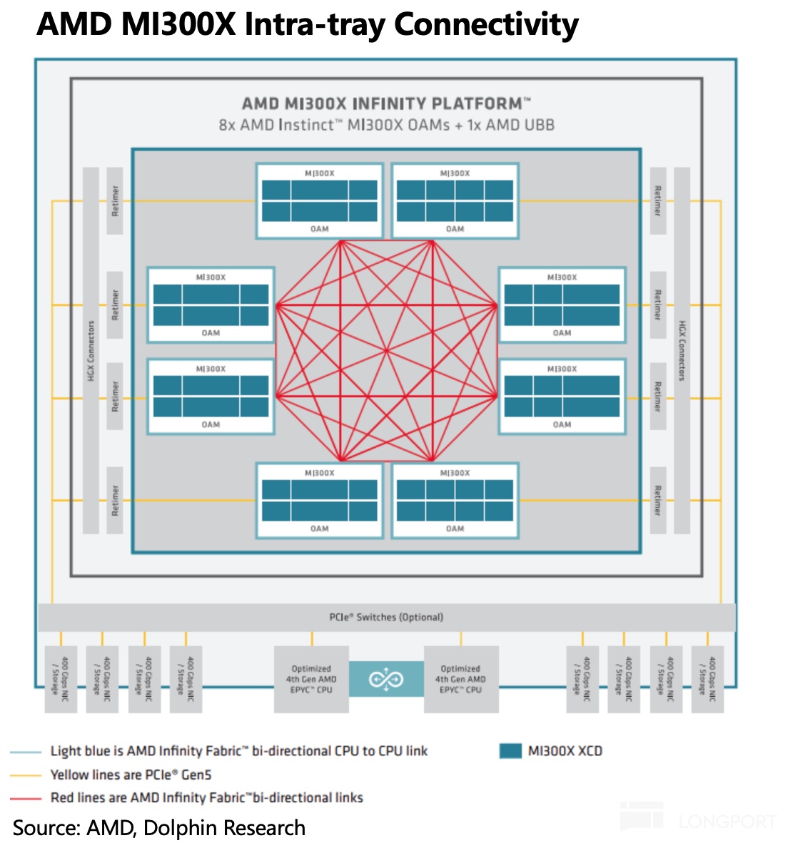
Before Helios (MI450 platform), AMD mainly sold MI300 chips, with only simple on-board GPU links. It lacked a Scale-Up switch ASIC like NVIDIA’s NVSwitch to directly interconnect dozens of GPUs. The gap is obvious: with only on-board links, eight GPUs are fully meshed, but beyond eight, inter-GPU traffic must exit to the Scale-Out network, degrading bandwidth and latency.
As noted earlier, it is like a team of eight in the same office can share files peer-to-peer. Once you exceed eight, files must hop person-to-person until they reach the final recipient.
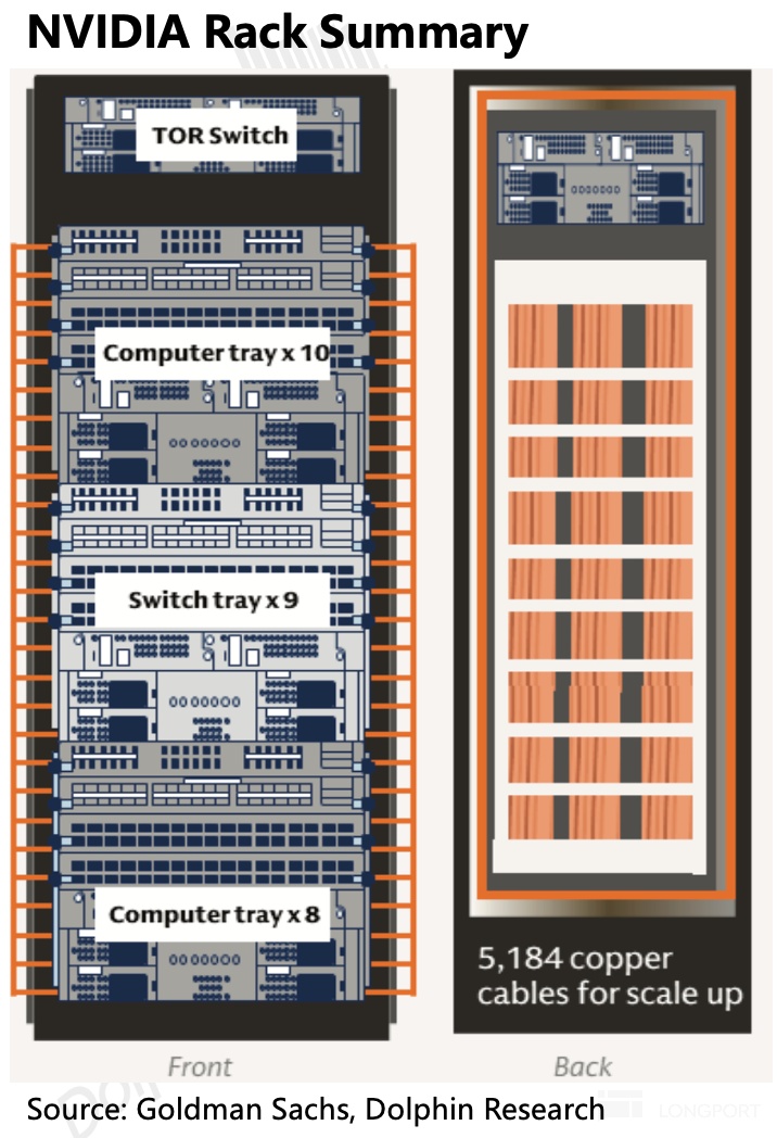
In NVIDIA’s GB racks, compute trays and switch trays make up the rack. As shown below, the front view places nine switch trays interleaved among eighteen compute trays, rather than at the top or bottom. It is akin to a central dispatch floor. You drop materials there, dispatch parses them, then one-hop routes them to the target recipient, enabling frictionless communication within 72 nodes.
For both training and inference under trillion-parameter models and MoE, the ability to aggregate as many GPUs as possible is the core differentiator. This left AMD’s MI300 generation unable to compete with NVIDIA’s GB racks, especially for training. AMD only earned a seat at the table once Helios (MI450) introduced a rack solution comparable to GB300.
Beyond CUDA’s strong ecosystem, a key NVIDIA trump card is the GPU Scale-Up fabric stitched by NVLink.
2.2 What sets NVIDIA GB300 apart: NVLink-centric GPU Scale-Up
To break the limit on the number of interconnected GPUs, NVIDIA added an NVLink-based switch ASIC, NVSwitch, between GPUs. NVSwitch connects all eighteen compute trays, each with four Blackwell GPUs, so that when the 72 GPUs exchange data, each sends to NVSwitch and the switch forwards in a single hop to the target GPU.
Specifically, a GB300 hosts eighteen compute trays (72 GPUs), ten trays above and eight below, with nine switch trays in the middle holding eighteen NVSwitch 5 ASICs. Each GPU exposes eighteen links into eighteen NVLink 5 switch ASICs. Per GPU, aggregate bidirectional bandwidth is 1.8 TB/s. Each NVSwitch has 72 ports and fully loads all GPUs, achieving single-hop, non-blocking, full connectivity between any two GPUs.
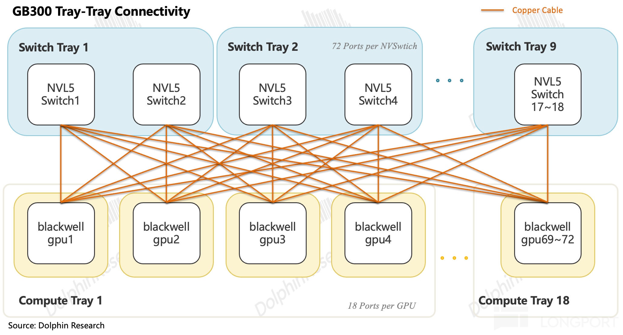
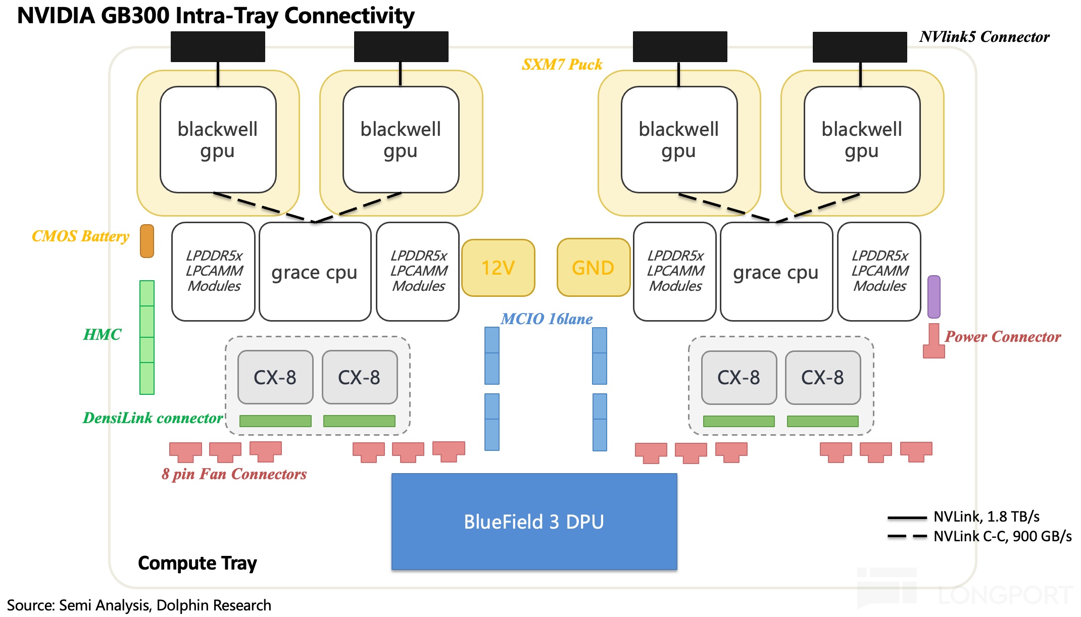
Regardless of proximity, two GPUs do not directly wire to each other. Signals traverse tray PCB tracks to edge connectors, go through the backplane connectors and copper cables into the switch tray connectors and flywires to the NVSwitch ASIC. In each tray, there are also two CPUs, and CPU–GPU uses NVIDIA’s NVLink C2C, not generic PCIe, delivering 900 GB/s bidirectional bandwidth.
2.3 AMD’s homework: what was copied, how close is it?
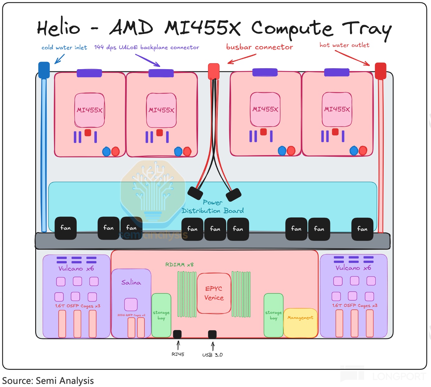
Helios mirrors GB300 in interconnect logic, introducing switch trays to tie 72 GPUs across 18 trays. The rack uses six switch trays and twelve switch ASICs, also over a copper backplane. Because its switch has more ports in use, per GPU bidirectional bandwidth reaches 3.6 TB/s, twice GB300.
But the real-world implementation differs meaningfully:
a. Protocol: While GPUs indeed Scale-Up via a switch, the protocol is UALoE over Ethernet, not native UALink. b. Switch silicon: Off-the-shelf third-party parts. Helios uses $Broadcom(AVGO.US) Tomahawk 6, a general-purpose switch typically used for Scale-Out. In Helios’ Scale-Up, there are unused ports.
Each Helios switch tray has four connector groups totaling 864 lanes, with two TH6s using 432 each, while a single TH6 can expose 512, leaving ~16% switch capacity idle, whereas NVIDIA fully utilizes its ports. In addition, constrained by weaker SerDes on-tray, Helios adds Ethernet retimers, raising cost, power, and assembly complexity.
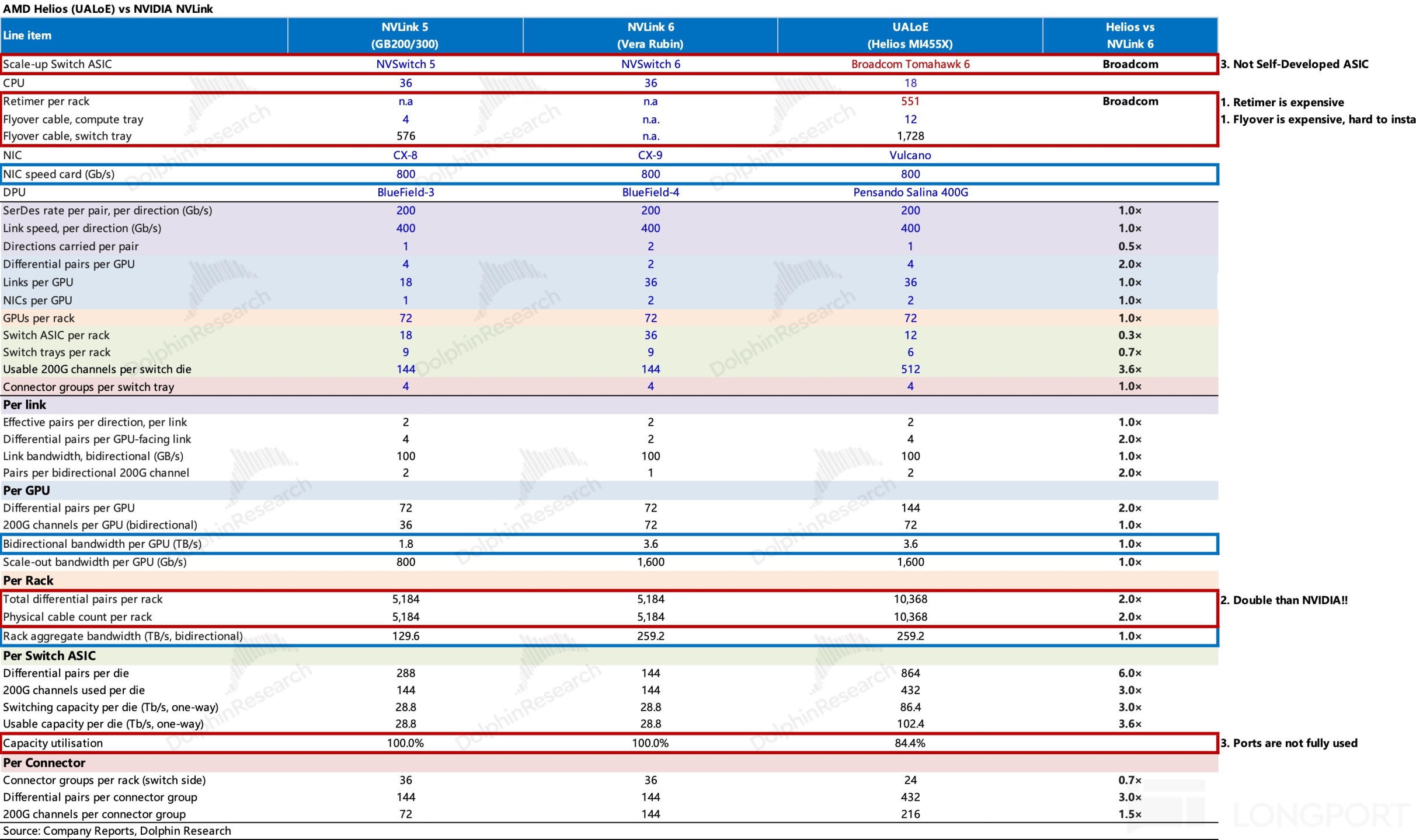
c. Twice the copper inventory: 10,368 copper cables in total, double NVIDIA’s count. The difference stems from NVIDIA’s SerDes supporting simultaneous bidirectional traffic on the same DP pair. d. Medium: still using copper flywires. The connector-to-switch segment retains GB300’s flywire design, adding cost and maintenance risk.
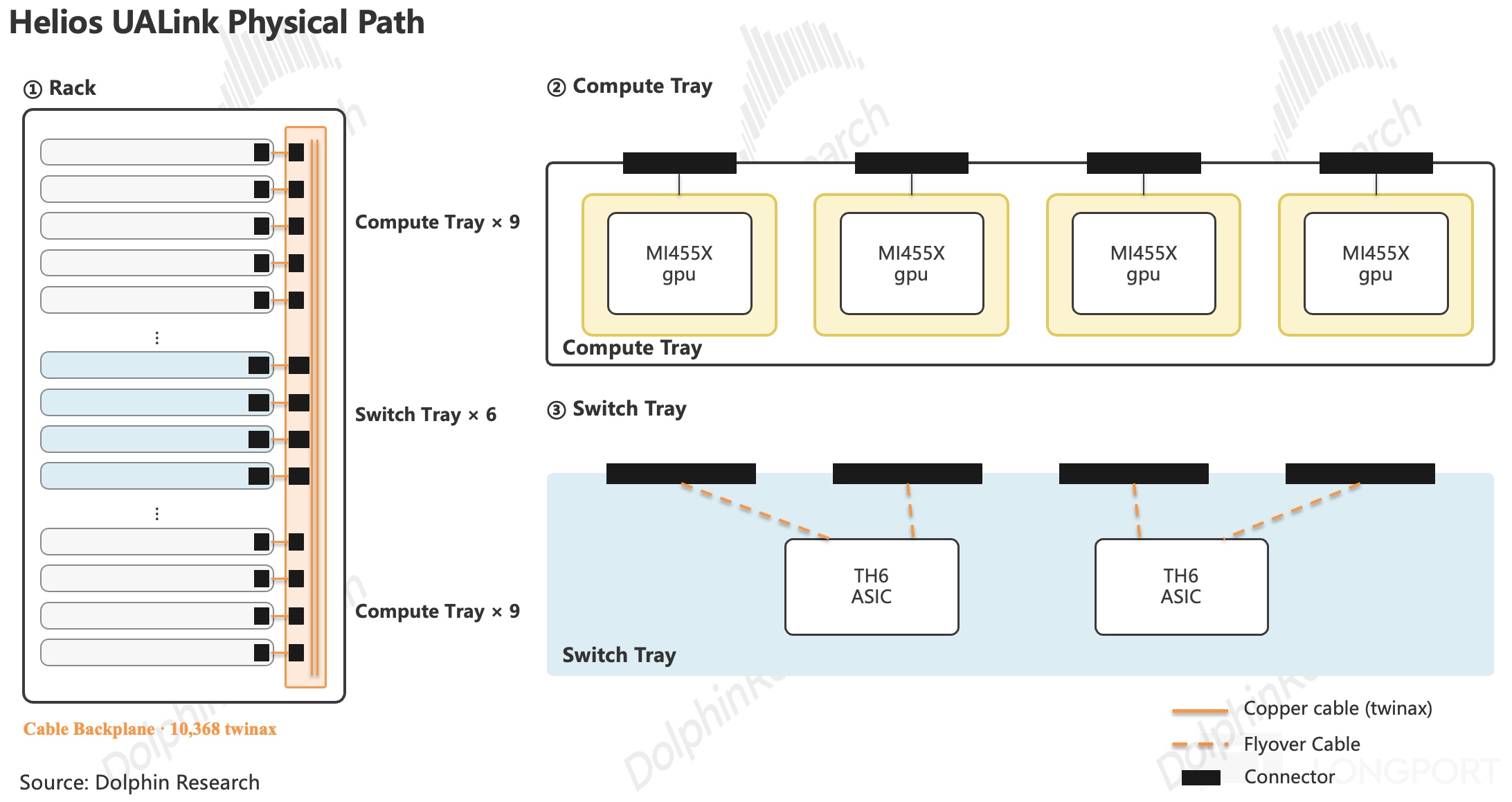
e. Lower CPU ratio; CPU–GPU again linked via flywires: Each compute tray has one Venice CPU and four MI455X GPUs, cutting the CPU:GPU ratio from NVIDIA’s 1:2 to 1:4. Because the CPU is farther from the GPUs, Helios links the Venice CPU and Pensando Vulcano NIC via flywires, rather than NVIDIA’s NVLink C2C.
From the protocol bandwidth chart below, AMD’s lower CPU ratio likely reflects NVIDIA’s NVLink C2C (1.8 TB/s), which brings CPU and its memory into the GPU coherence domain, requiring higher CPU count. AMD’s CPU–GPU uses IF at only 256 GB/s. The CPU may primarily handle control and scheduling, making one CPU sufficient for four GPUs.
2.4 Helios’ true peer: what did Vera Rubin iterate?
Flywires are consumables prone to failure and hard to repair. Vera Rubin’s key update is eliminating flywires, upgrading to 36 NVLink 6 switch ASICs, and raising GPU-to-GPU bandwidth to 3.6 TB/s. It also doubles CPU–GPU NVLink C2C bandwidth to 1.8 TB/s.
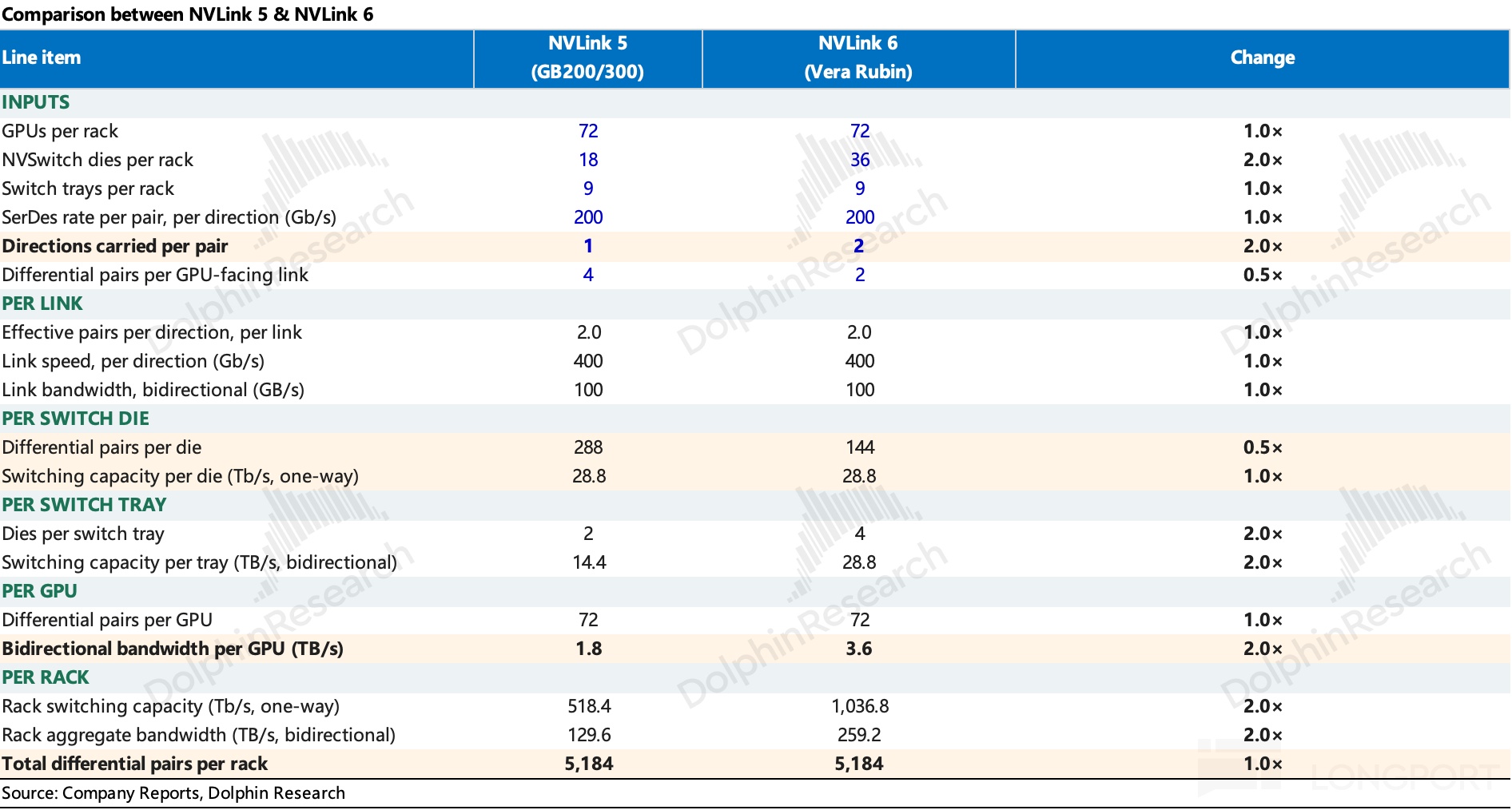
The key is how flywires were removed.
In GB300, the compute tray centers on a highly integrated PCB hosting GPU, CPU, and LPDDR. The signal path out of the chassis is CPU → GPU → NIC → OSFP → leaf switch. The NIC-to-OSFP segment uses flywires (blue dashed line on the left), which was the most failure-prone link.
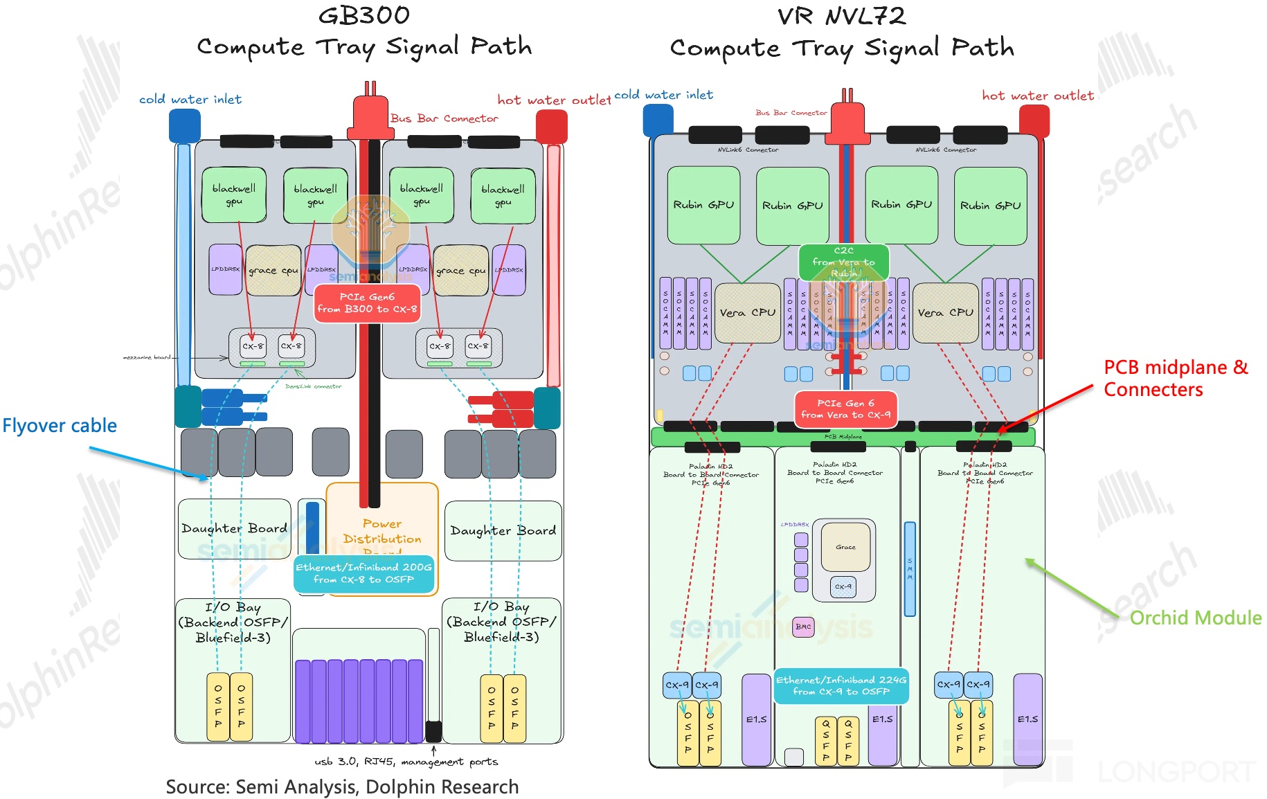
Vera Rubin’s solution is modularizing the boards. CPU and GPU form the compute module, and CX-9 lines up next to the OSFP ports within a standalone network module named Orchid. These modules interface via a vertical PCB midplane. Modules no longer use cables, but blind-mate via board-to-board connectors (red arrows on the right), simplifying maintenance and assembly.
After blind-mating, the entire path is PCB routing. Long PCB runs attenuate more than flywires, so NVIDIA complemented high-speed SerDes with upgrades to PCB material, layer count, and area.
From GB to Vera Rubin, the GPU interconnect topology stays the same. The change is modularization plus PCB midplanes and connectors replacing flywires, cutting assembly time and easing maintenance. Helios copies NVIDIA’s prior-gen design and boosts headline specs with higher-cost components, but non-custom parts and design choices drive higher actual cost. Its direct competitor is NVIDIA’s improved Vera Rubin.
2.5 Scale-Out: no core differences
This layer is simpler, focused on more hardware and higher bandwidth. We compiled an overall comparison table based on the Scale-Up analysis above. Light red cells mark where AMD lags NVIDIA.

2.6 What’s next for NVIDIA: is Rubin Ultra another major overhaul?
NVIDIA is maturing Rubin Ultra, the successor to Vera Rubin, which may introduce optical Scale-Up across racks for the first time. Two rack styles are being evaluated in parallel: Kyber vs. traditional Oberon.
a. Kyber rack (NVL144, left): redesigning the form factor
Compute trays become vertical blades mounted along two large PCB midplanes. Each blade integrates four Rubin Ultra GPUs and two Vera CPUs, and the rack is split into two full-function canisters, each holding eighteen blades, for a total of thirty-six blades and 144 GPUs. On the midplane’s opposite side, switch capacity scales up. Each switch blade has six NVLink 7 switch ASICs, twelve per rack, totaling seventy-two. GPUs fully mesh across the two PCB midplanes, and a management module is added.
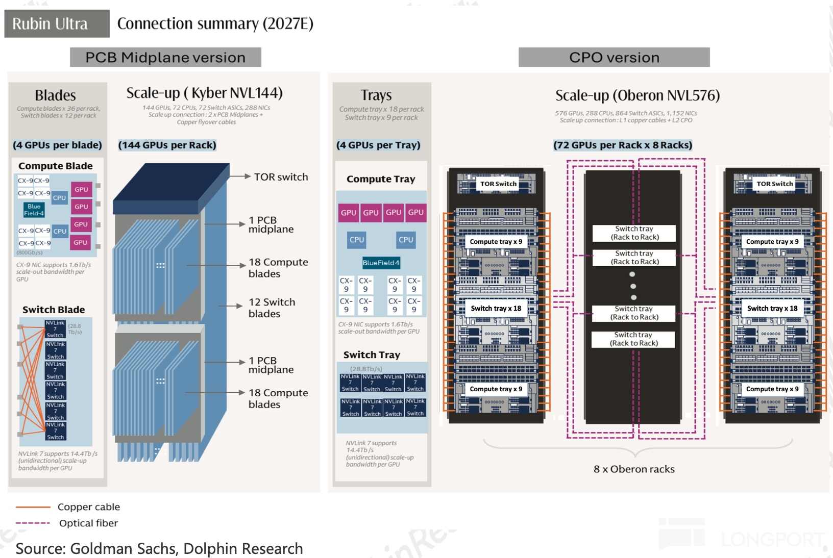
b. Oberon rack (right): keeping horizontal trays
i) In-rack layout changes from Vera Rubin’s 10+9+8, with nine switch trays in the middle, ten compute trays on top, and eight below. The new plan shifts to 9+18+9. The eighteen compute trays split evenly between the top and bottom, NVLink switch trays double to eighteen, and each tray’s height compresses to 0.75U, shortening the longest compute-to-switch path to maintain NVLink drive over the copper backplane.
ii) Cross-rack, optical Scale-Up lifts the ceiling. Eight racks, each with seventy-two GPUs, will use Scale-Up CPO for load/store memory semantics across racks, rather than RDMA message semantics typical of Scale-Out.
III. Takeaways: seat at the table in theory, still a perpetual backup in practice
On headline bandwidth, Helios largely matches NVIDIA at both Scale-Up and Scale-Out. Per GPU bidirectional Scale-Up reaches 3.6 TB/s, comparable to Vera Rubin, and Scale-Out uses 800G NICs. For customers, AMD now meets the baseline to be a viable alternative.
But matching theoretical bandwidth is not enough. AMD’s gaps lie in engineering execution and a self-developed full stack. By retaining GB-era design elements, Helios pushes up rack-level BOM costs.
Based on our estimates, even if we assume aggressive CPO adoption on NVIDIA’s Scale-Out side that lifts its cost, AMD’s physical network layer cost per rack (external procurement) is still close to double. The spread is mainly in Scale-Up: twice the copper cables, plus off-the-shelf switch ASICs and retimers account for ~60% of Helios’ Scale-Up network cost.
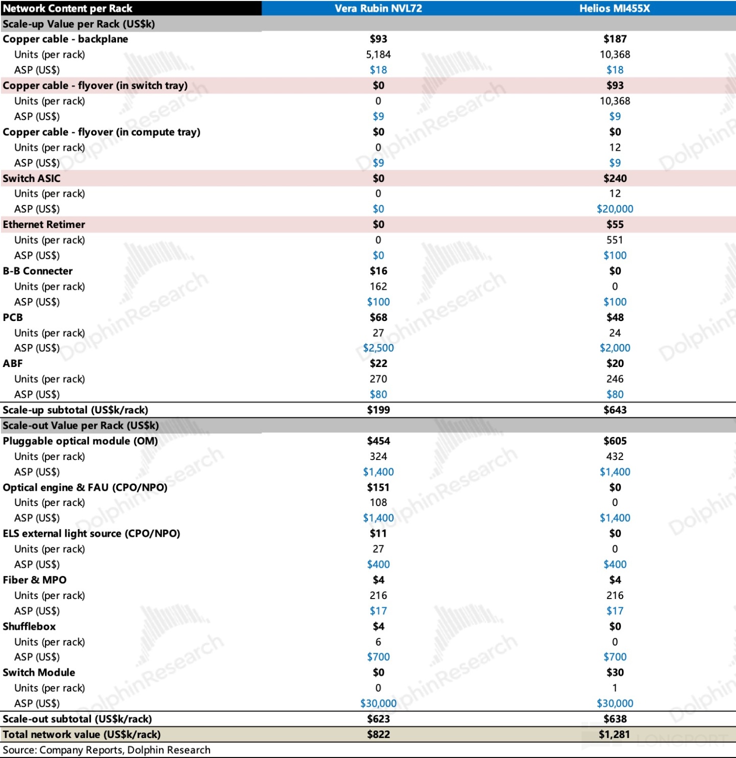
As a challenger, AMD will likely price more aggressively to win orders, ignoring rack storage differences. The gap we detailed will show up in rack solution gross margins.
Because Helios relies heavily on third-party components, AMD’s retained revenue is mainly GPUs (Instinct MI455X), CPUs (EPYC Venice), and NICs (Pensando Vulcano. Other elements are largely low-margin resale. At the rack-level interconnect contest, AMD is constrained by the slow path to native UALink and its follower stance, while NVIDIA’s racks keep iterating and may even change physical form in the next generation.
AMD’s solution still trails NVIDIA meaningfully. Yet with compute scarce, AMD is entering an upcycle. Management has said demand for 2027 is already above initial expectations and will keep adding capacity.
IV. Value chain mapping: inside the rack, boards replace cables; outside, optics replace copper
From deployments and orders won downstream, Vera Rubin began volume shipments in Aug and has orders from all major hyperscalers, AI cloud providers, and system OEMs. The market generally expects a 4Q26 ramp.
Helios entered mass production in late Jul, with first shipments by end-Sep. It lags volume commercialization by roughly one quarter, with broad ramp likely in H1 2027. Public data on AMD’s supply chain is limited, but both racks converge on similar hardware specs (3.6 TB/s, 200G SerDes, copper backplane plus multi-layer PCB), and the competitive landscape at key nodes is concentrated.
In baseplates, PCB, liquid cooling, and PSUs, supplier overlap is high. The main differences are: i) AMD uses Broadcom switch silicon, and ii) for system integration, NVIDIA uses Foxconn and Quanta, while AMD works with Sanmina, Celestica, and HPE, i.e., more U.S.-centric integrators.
Below we summarize how interconnect suppliers’ value shifts through rack solution comparisons and iterations.
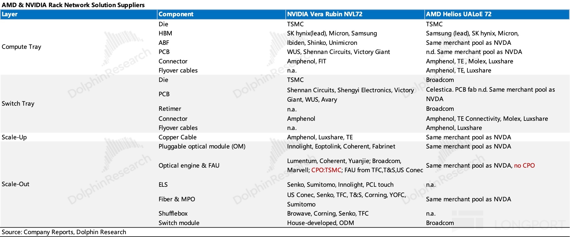
4.1 Winners and losers through iterations
a. AMD chain: Helios extends AMD from eight GPUs per board to seventy-two across boards. The switch trays and Scale-Up layer are the clearest incremental drivers. Broadcom supplies Ethernet retimers and switch ASICs for switch trays, and $Amphenol(APH.US) provides end-to-end copper interconnect solutions. Both are direct beneficiaries.
Longer term, native UALink switch silicon will come from $Marvell Tech(MRVL.US) and $Astera Labs(ALAB.US), substituting Broadcom in Scale-Up. Also, Google’s OCS switches are conceptually designed as substitutes for Broadcom spine switches.
b. NVIDIA chain: copper out, PCB and optics in; connectors upgraded
NVIDIA’s rack interconnect changed in two key ways: first, compute-to-switch flywires were eliminated, and second, PCB area and rigidity were increased. Based on physical cost estimates, Vera Rubin’s overall interconnect cost is ~1.8x GB, but per-card bandwidth doubled. On a per-bandwidth basis, network cost actually dropped ~10%.
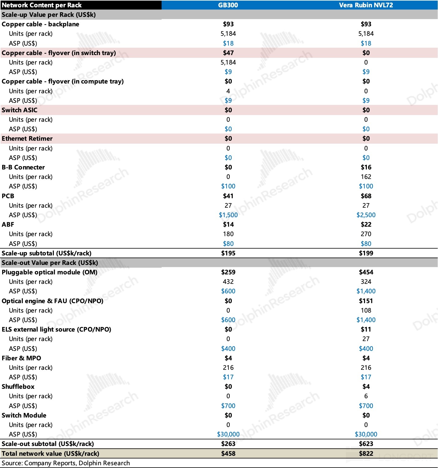
Connectors: mixed impact for Amphenol. Removing flywires (passive copper) is a headwind for Amphenol. The offsets are higher ASP and more ports for on-tray connectors. The copper backplane solution (incl. connectors) remains primarily supplied by Amphenol, so net impact is neutral.
PCB sees both volume and price tailwinds. Volume rises with larger clusters driving rack count. Price benefits from materials upgrades, higher layer counts, and more complex boards. Over a longer horizon, Kyber racks will replace in-rack copper cables with PCB midplanes, further helping PCB vendors at the expense of copper interconnect.
4.2 Interconnect value distribution: who captures more?
Per rack BOM, we group all network materials into four buckets, from higher to lower value: optical interconnect (modules and optics) > switches > copper interconnect (cables and connectors) > PCB and ABF.
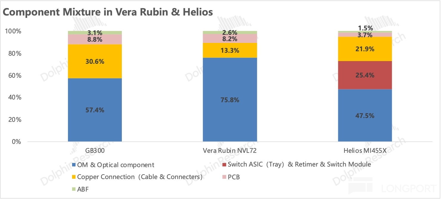
1) Optical interconnect: supply-demand mismatch driven pricing; sustainability is uncertain
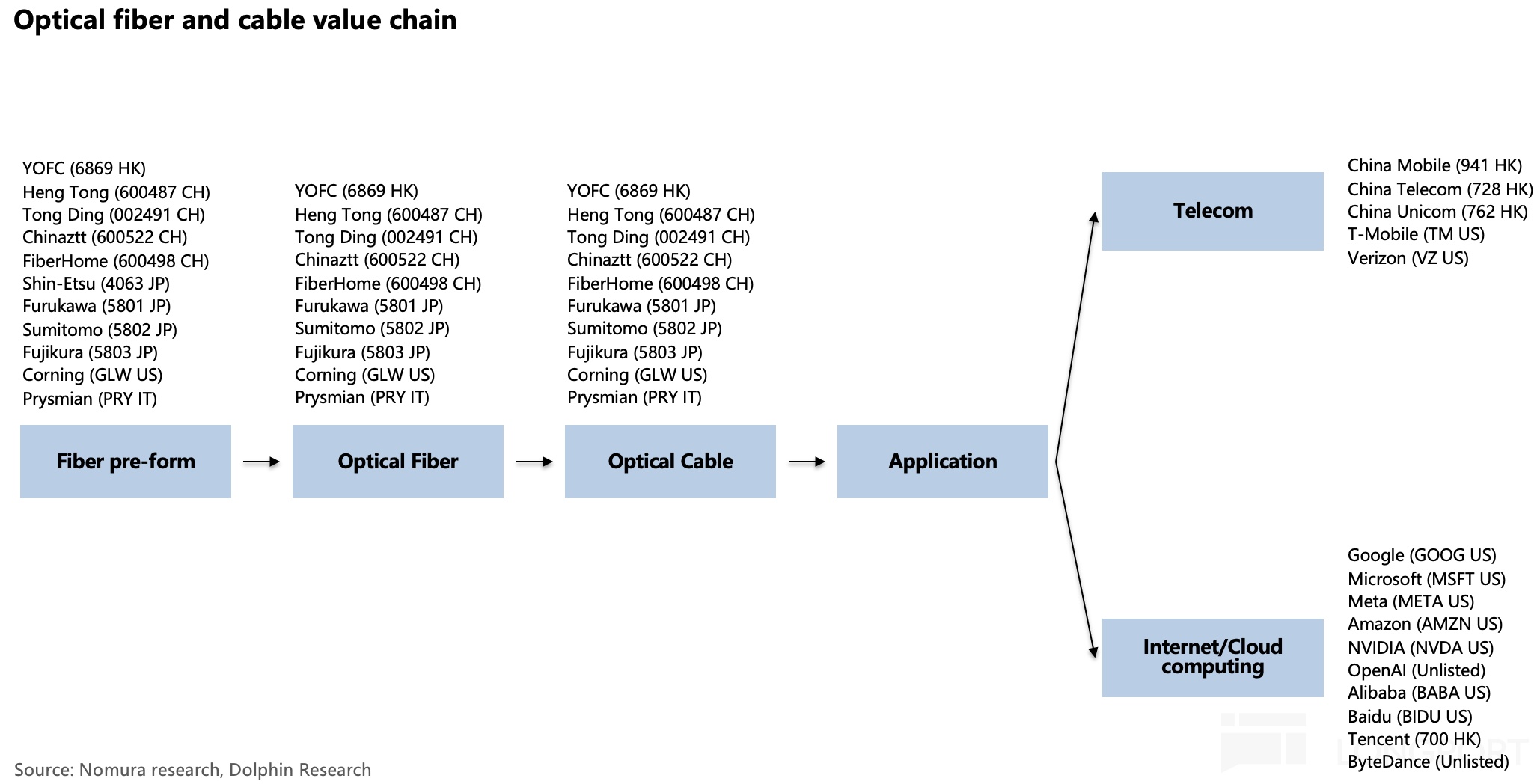
We have covered optics in depth; cf. technology roadmap and value chain mapping. Here we add the fiber cable chain.
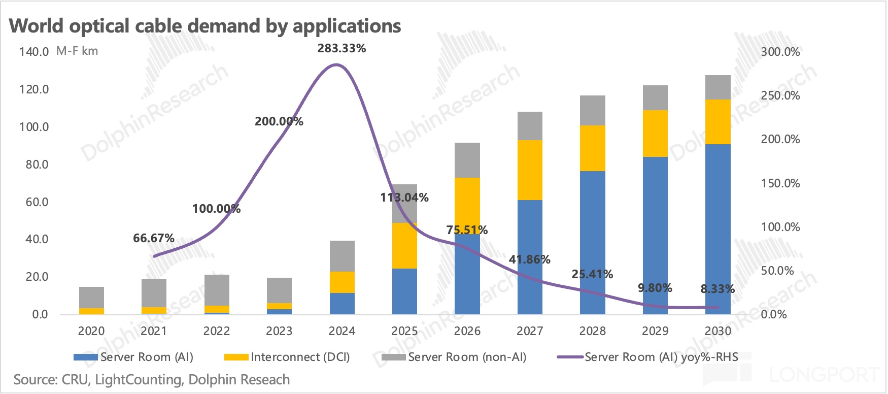
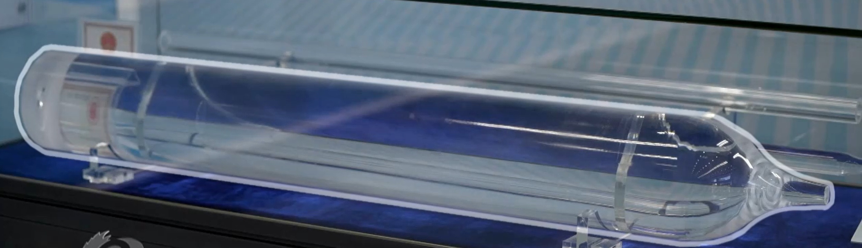
Price hikes stem from a supply-demand mismatch. Demand is structurally higher as AI clusters scale, while supply is constrained upstream at the optical fiber preform stage, an ultra-pure solid quartz glass rod. Preforms define the fiber’s optical DNA, are drawn into bare fiber, then jacketed to form finished fiber.
Preforms command the most value, contributing ~70% of chain profits, and require the most exacting equipment and process.
Mature capacity is led by $Corning(GLW.US), Fujikura, and $YOFC(06869.HK), most of which is not sold externally. Incumbents are cautious on expansion, and with 18–24 months needed to add capacity, supply is rigid. The shortfall cascades downstream, driving broad price increases over the past year.
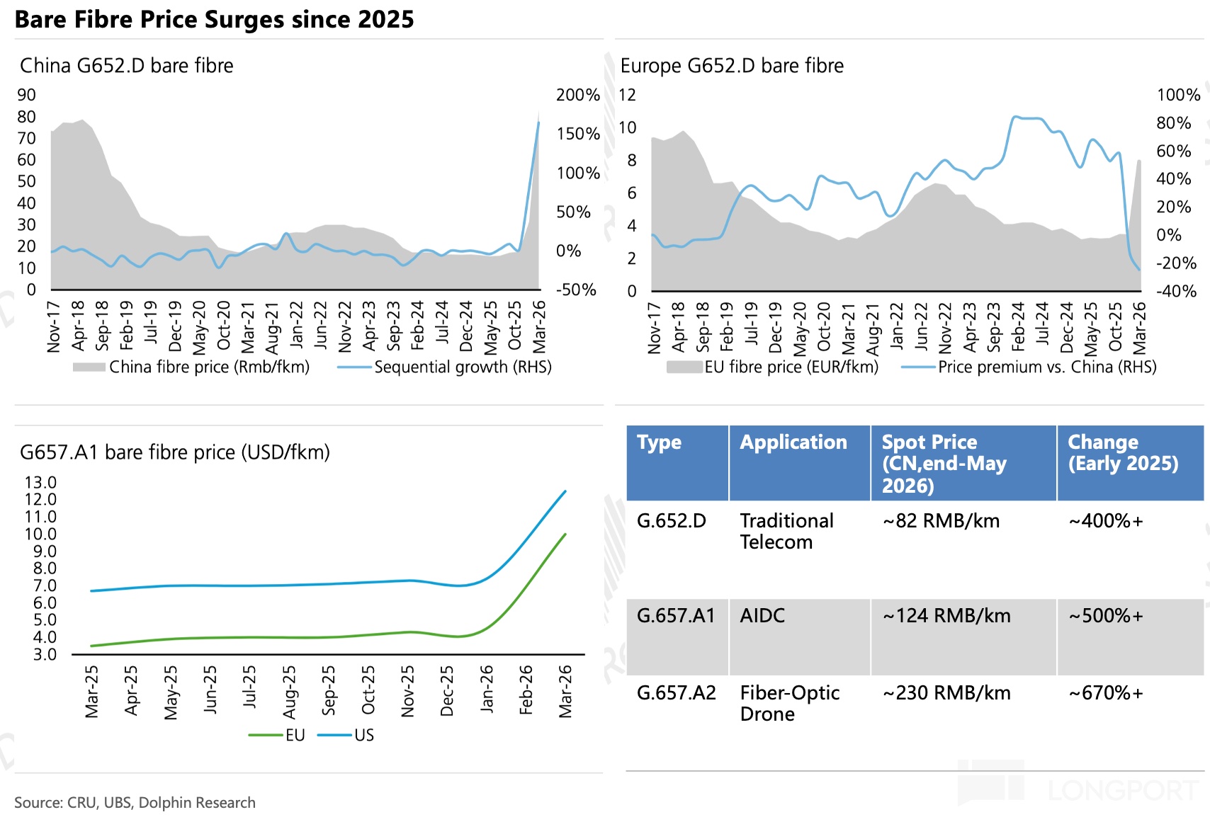
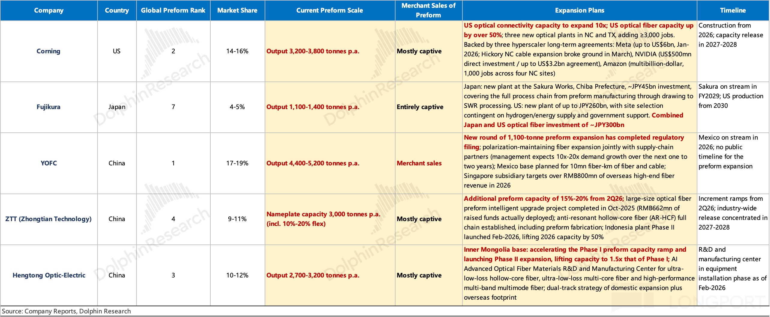
Durability of price hikes is questionable. While preforms were long seen as a high-barrier segment, newcomers are scaling aggressively. Han’s Laser plans +2,000 tons and Hesheng Silicon +3,200 tons, with capacity landing in H2 2027. Competition in China is already intensifying. As of Jun, G.657.A spot prices ticked up MoM, while G.652.D was flat. New tech like HCF (hollow-core fiber, led by YOFC) remains early, at ~0.02% of annual fiber shipments, and is less deterministic than CPO for driving broad industry upgrades.
In segments with some but not insurmountable barriers, vertical integration matters. We suggest focusing on leaders with captive preform or full-chain integration, such as YOFC, Corning, and $HTGD(600487.SH), which should benefit from pricing power and cost advantage as capacity normalizes.
2) Switching: self-developed for Scale-Up; procurement-heavy for Scale-Out
At Scale-Up, the industry is moving toward self-developed switch ASICs on switch trays. This is the ideal path for tight coupling with self-developed protocols, and the drawbacks of generic switch silicon were evident in Helios. At Scale-Out, procurement still dominates. In our upcoming CSP interconnect deep-dive, despite self-development across layers, hyperscalers still rely on Broadcom, Marvell, and NVIDIA for high-end switch silicon, given durable moats in SerDes IP, protocol co-design, and software stacks.
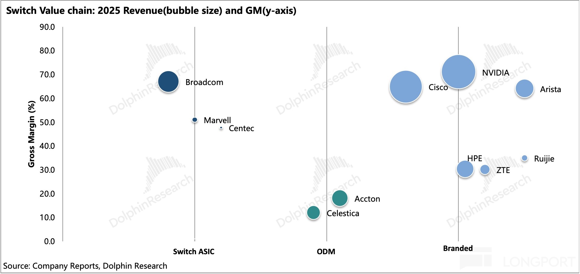
Switch ASICs carry the highest technical and value density in the switch chain. Bernstein estimates ASICs at ~30% of switch module value. The market is highly concentrated: Broadcom ~70%, with Marvell and NVIDIA at ~15% and ~10% respectively.
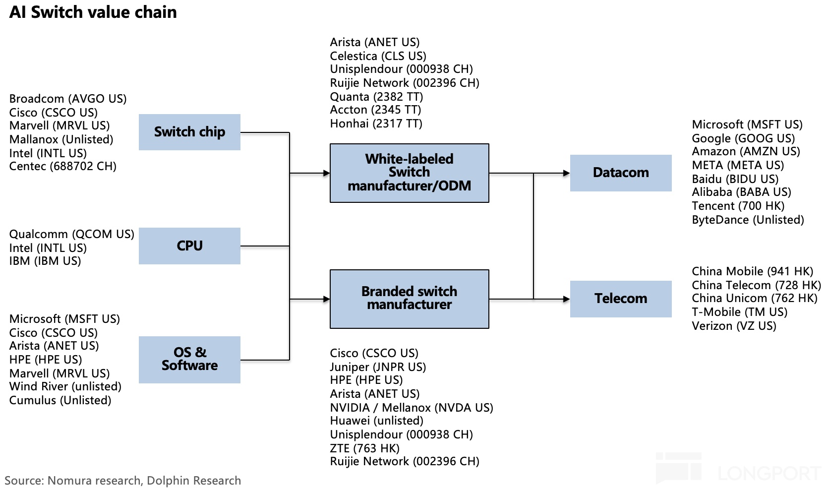
Switch ASIC gross margins are ~50–70%. Branded switch leaders (Arista, Cisco, NVIDIA) run >60% GM, far above white-box ODM at 10–20%. We therefore favor high-end silicon and branded switch vendors with pricing power: Broadcom, Marvell, $Cisco(CSCO.US), NVIDIA, and $Arista Networks(ANET.US).
3) Copper interconnect
Both NVIDIA and AMD use DAC for backplane copper, which is range-limited and unsuitable for cross-rack Scale-Up. AEC may extend copper’s lifecycle, and we will discuss it in AWS’s value chain, where AEC is a major adoption theme.
4) PCB and ABF
a. PCB/HDI: Japan controls materials; value accrues to high-layer boards
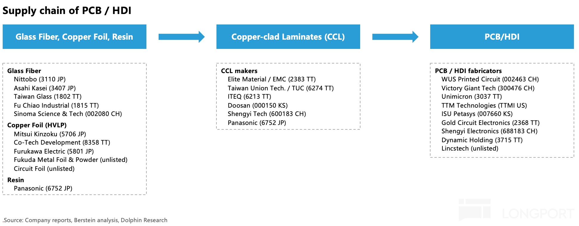
CCL is the core of PCB/HDI, at ~30% of PCB cost. CCL cost is concentrated in three upstream materials: copper foil ~40%, resin and glass fabric ~25% each.
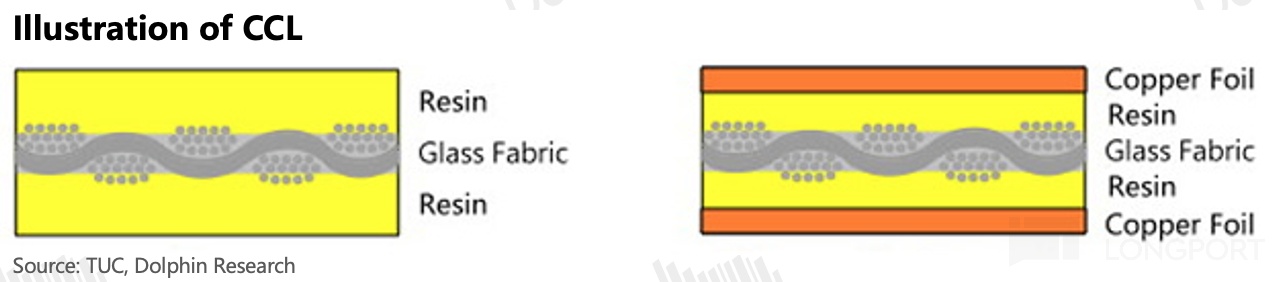
PCB makers’ cost and bargaining power hinge on two high-end materials: glass fabric and copper foil. VR removes NVLink flywires in favor of long PCB runs, demanding ultra-low dielectric loss (Dk for delay, Df for loss) and extremely smooth copper. This generation requires low Dk/Df glass fabric and HVLP copper foil.
Supply is concentrated: third-gen low-Dk glass fabric is dominated by Nitto and AGC. Second-gen fabric is undergoing domestic substitution but still mainly ships from Nitto, AGC, and Taiwan Glass. HVLP4/5 copper foil is >80% supplied by Mitsui.
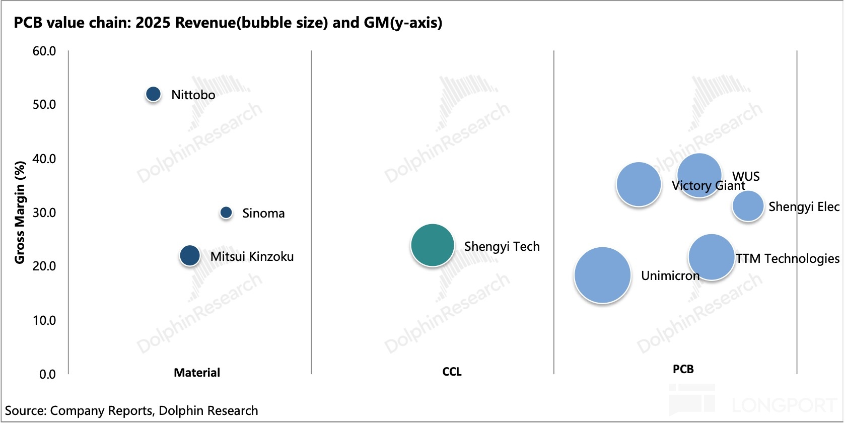
On manufacturing, the market expects Rubin Ultra backplanes to reach 78+ layers. Shenghong has 70+ layer mass production and 100+ layer R&D, while Shennan Circuit can mass produce 68 layers and has 120-layer reserves. Upstream tightness aside, margins across the chain sit at ~30–40%, suggesting price increases can pass through and are not solely captured upstream.
We recommend leaders with high-layer mass production capability: $VGT(02476.HK) and $SCC(002916.SZ).
b. ABF substrates: Japan and Taiwan dominate
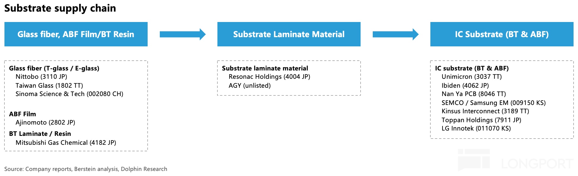
ABF substrates used in AI accelerators have fewer layers but must remain stable under high temperatures, requiring more demanding process control. The market is concentrated: the top three players (Ibiden, Unimicron, SEMCO) account for over 50% share.

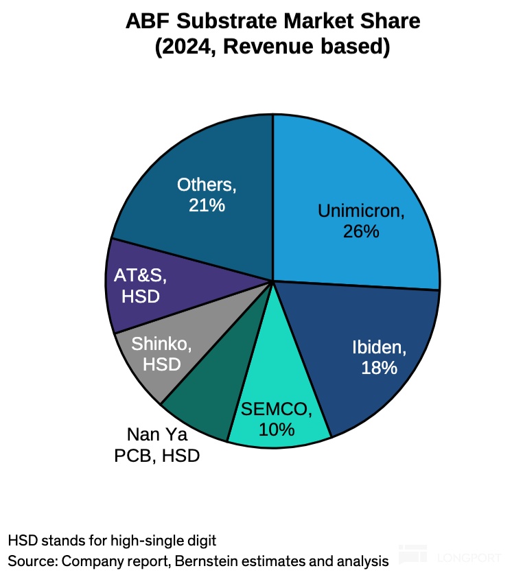
Upstream materials are largely monopolized by Japanese firms.
- T-glass (low-CTE glass fiber): Nitto holds ~90% global share, effectively a monopoly.

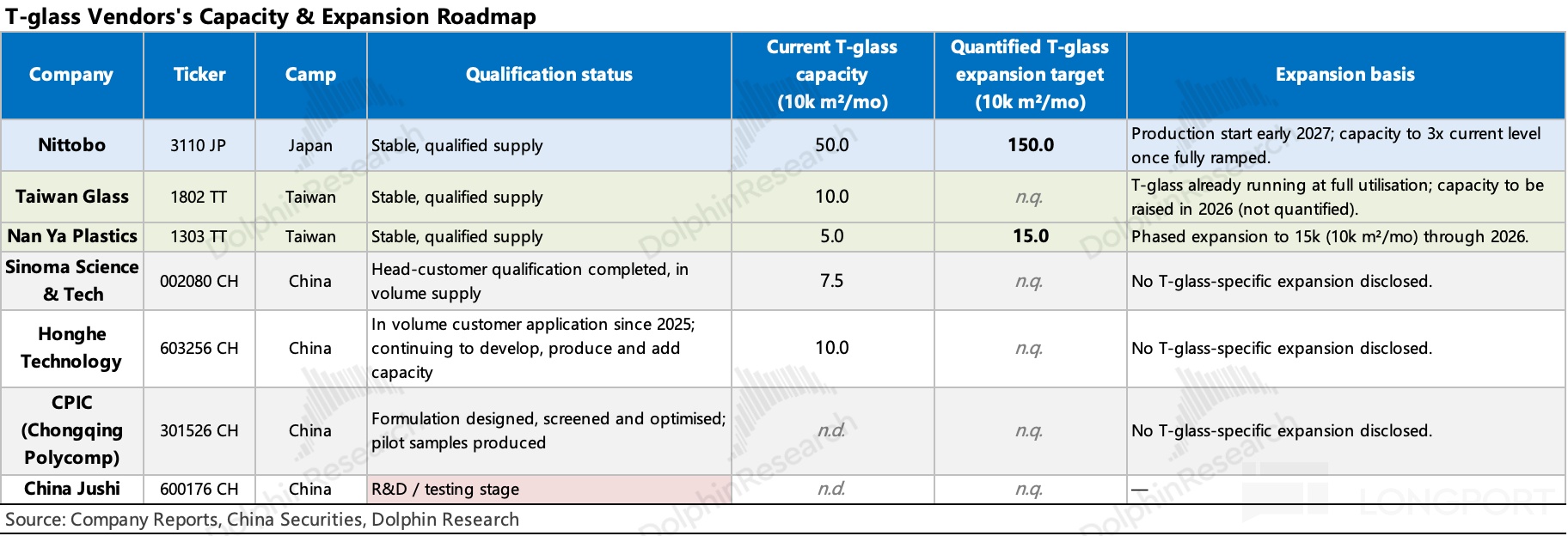
- ABF build-up film: Ajinomoto holds 95–98% share, with >2 mn sqm monthly capacity. It was fully utilized by Q2 2026, and new capacity will only land in 2030–2032, keeping supply rigid near term.
We summarize core assets in AI DC interconnect below.
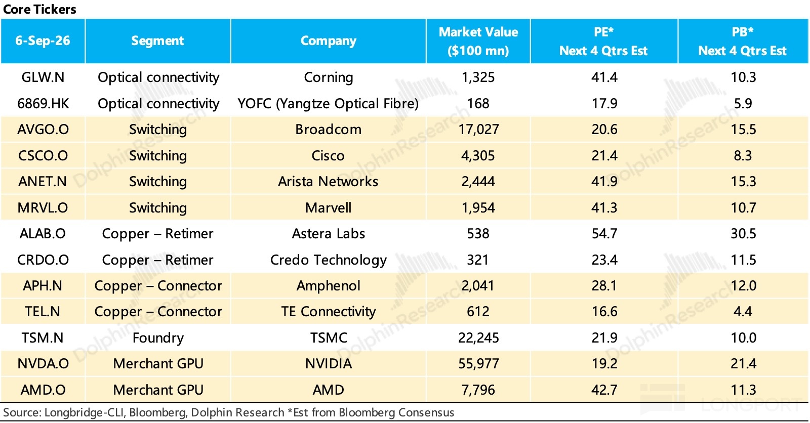
After comparing network solutions from Google, AWS, and Huawei, we will highlight and track the key assets across the value chain. Stay tuned.
<End>
Risk disclosure and statements: Dolphin Research disclaimer and general disclosures
Dolphin Research AI DC interconnect series:
‘AI in the hyperconnect era: racing toward optics?’
‘Copper stays: CPO, real opportunity or mirage?’
‘AI-era DC interconnect: cluster-first beyond single chips; is there a China angle?’


The copyright of this article belongs to the original author/organization.
The views expressed herein are solely those of the author and do not reflect the stance of the platform. The content is intended for investment reference purposes only and shall not be considered as investment advice. Please contact us if you have any questions or suggestions regarding the content services provided by the platform.