

MUU
28.3000.57%
D
1 day ago, 12:47 PM
AI inferencing boom: Can beleaguered WDC rise from the ashes?
 I'm LongbridgeAI, I can summarize articles.
The AI upcycle has turned NAND from a cyclical, over-supplied commodity into a scarce strategic resource. After the split, shedding the drag from legacy HDDs, Sandisk made a pure bet on NAND and data center SSDs, catching the right wave.
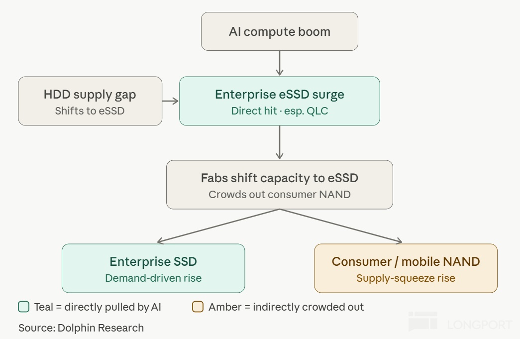
AI servers need to read and write historical data at high frequency when doing inference, handling complex tokens and prompts, processing multimodal inputs (video, images), and generating synthetic data. Traditional cloud storage configurations can no longer keep up, and per-node NAND consumption on AI servers is growing exponentially.
During the training-led phase, vendors prioritized compute horsepower. As we shift to inference, 'AI infra = XPU + storage + interconnect', compute matters a bit less while demand tilts toward storage and connectivity.
How does AI infra reshape overall NAND demand? In practice, AI data centers do not need the full NAND product stack, with demand concentrated in enterprise SSDs. In the Agentic AI and large-scale inference era, the most sought-after parts are ultra-high-capacity enterprise QLC SSDs and PCIe 5.0/6.0 SSDs offering high bandwidth and low latency.
As large CSPs bid up enterprise SSDs with high premiums and long-term orders, suppliers are shifting capacity away from phones and PCs to AI-grade enterprise products. This supply-side squeeze is indirectly tightening the broader NAND market balance, lifting the overall cycle.
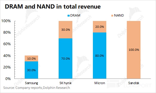
The main NAND players are Samsung, SK hynix, Micron, and Sandisk, with Sandisk being the purest play. The three memory majors still center on DRAM and HBM, while Sandisk, post-HDD exit, is fully focused on NAND and thus stands to benefit most from this NAND upcycle.
For Sandisk, Dolphin Research addresses three questions here: (1) Sandisk’s relationship with Western Digital; (2) its partnership with Kioxia; (3) how Sandisk’s NAND tech stacks up. We will cover results and valuation in the next note, stay tuned.
On technology strategy, Sandisk does not chase layer counts at all costs, instead pushing lateral scaling to achieve top-tier bit density. It was first to mass-produce the CBA bonding architecture to boost performance and efficiency, and co-introduced HBF (High Bandwidth Flash) for AI inference, keeping it in the leading cohort among NAND makers.
With AI inference driving a surge in ultra-high-capacity enterprise QLC SSD demand, Sandisk benefits from secured capacity with Kioxia through 2034, high earnings elasticity as a pure-play NAND, and optionality from HBF. The company should continue to enjoy AI infra tailwinds.
Dolphin Research’s in-depth look at Sandisk (SNDK.O) follows below:
I. Sandisk and Western Digital: a decade-long itch, separation benefits both
What kind of company is Sandisk? Though newly listed, Sandisk is a storage veteran founded in 1988 and a pioneer in flash, acquired by Western Digital in 2016 for about $16bn. The roots run deep in the storage industry.
HDD and NAND differ materially in growth and development logic, which led to a conglomerate discount for the combined entity. In Oct 2023, Western Digital announced a plan to spin off its flash business into a new listed company under the Sandisk name, with WDC focusing on HDDs and re-listing separately in Feb 2025.
At the time of the spin, Western Digital retained 19.9% of Sandisk, cutting that to around 5% by Jun 2025. When WDC bought Sandisk, it raised roughly $18bn of M&A debt, leaving the company under a heavy debt load for nearly a decade.
As Sandisk’s stock kept rallying, WDC sought to monetize its stake to reduce leverage. In a Feb 2026 filing, WDC said it planned to dispose of all 7.5mn Sandisk shares, which could trim over $3bn of debt.
WDC executed the 7.5mn-share disposal in two steps. First, it offloaded 5.82mn shares via a debt-for-equity swap followed by a secondary offering, bridging the redemption of all senior notes, converting debt to equity, then selling through the underwriting banks. Second, it swapped the remaining 1.69mn shares for its own stock and canceled the 4.8mn WDC shares received.
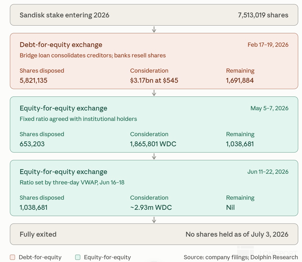
This separation benefits both parties. For WDC, it eases debt pressure and sharpens focus on HDDs; for Sandisk, it becomes a fully independent NAND and SSD company with clean governance. With equity ties severed, Sandisk has full control and no need to balance HDD priorities.
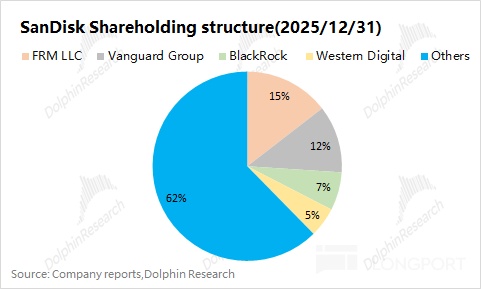
By end-2025, WDC was still among Sandisk’s top shareholders. As WDC exits its position, Sandisk becomes an independent tech company largely owned by Wall St. institutions such as Fidelity, Vanguard, and BlackRock, and the WDC overhang is gone.
II. Sandisk + Kioxia: a 20+ year partnership
Compared with peers like Micron, Sandisk’s portfolio is more singular, with all revenue from NAND. Early in this AI cycle, attention centered on HBM and Sandisk did not benefit, but as the storage cycle pivoted to NAND, an all-in NAND model delivered higher operating leverage.
Industry-wise, shipments are dominated by Samsung, SK hynix, and Micron, with Kioxia and Sandisk following and together holding roughly 15% share. The market is concentrated at the top.
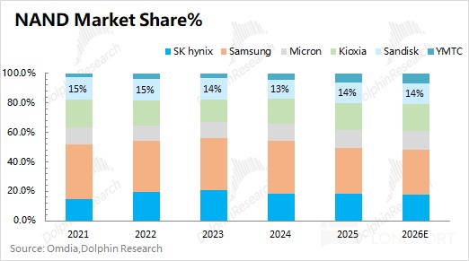
Sandisk and Kioxia have maintained similar market shares over time, and Sandisk’s wafer capacity largely comes from their Japan JVs. The two split wafer output, broadly on a 4:6 ratio, and sell independently.
Toshiba (Kioxia’s predecessor) invented NAND but lacked the capital and system integration for mass commercialization, while Sandisk had the tech and channels. Around 2000, they decided to build fabs together in Yokkaichi, Japan, forming a deep alliance.
They co-invested to purchase front-end equipment such as lithography tools, sharing heavy-asset risk. They co-developed the BiCS architecture in a shared lab up to the die, with post-die flow differentiated via each firm’s own design and firmware. On capacity, they split wafers roughly 50/50 at the front-end, each taking half and selling on their own.
The relationship has remained solid through Sandisk’s acquisition and relisting and Toshiba Memory’s rebrand to Kioxia. In Jan 2026, the partners extended the JV agreements from the original 2029 expiry to Dec 31, 2034, securing continuity.
On the same day, both announced BiCS10 engineering samples would be available in Jul 2026 with identical specs: 332 layers, 1Tb TLC, area density above 29 Gb/mm², a 59% uplift vs. BiCS8, and 4.8Gb/s interface speed (+33%). They continue to use the CBA and OPS features introduced at BiCS8.
Sandisk’s NAND wafers mainly come from two large bases in Japan. Yokkaichi is the world’s largest flash site with fabs from Fab 3 to Fab 7, while the Kitakami campus is the growth site with K1 and the newly ramped K2.
Kioxia announced on Aug 27 that site prep has begun for Kitakami Fab 3, located south of Fab 2. It targets start of production in FY2029 and will expand advanced BiCS FLASH capacity.
On the same day, the two companies said they plan to invest over $31bn (approx. JPY 5tn) in Japan by 2032, subject to Gov. support. The market expects K3 to account for about JPY 1.8tn (roughly $11.3bn).
III. 3D NAND stacking technology and economics
The transition from 2D to 3D NAND is less about process node and more about stacking layers. Capacity gains no longer rely on node shrink alone, but on higher layer counts, which breaks the process scaling dead end.
More layers translate directly into higher storage density, lifting output per wafer. This means NAND supply can rise with modest capex, and the progress in layer counts shows up in product capability and cost curves.
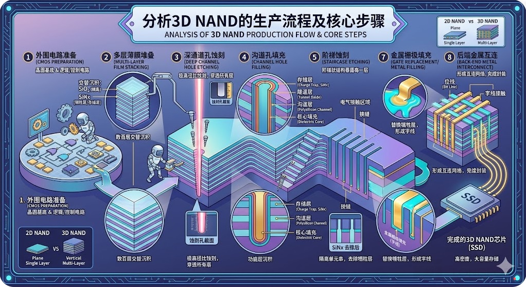
a) Stacking choices
As layer counts rise, the biggest challenge is deep channel hole etch. Specifically, one must drill billions of holes tens of nanometers wide through 200–300 stacked films with extreme vertical precision.
At 200–300 layers per single etch, the process approaches the physical limit. Think of piercing hundreds of sheets with a fine needle without bending or breaking, and keeping hole diameter tight at the bottom.
At 200+ layers, Micron, Samsung, and others mostly adopted dual-stack. They deposit 100–120 layers and etch once, then deposit another 100–120 layers and etch again to reach the total.
As the industry pushes toward 300 layers, Samsung and SK hynix diverged in approach. Samsung sought to extend dual-stack with material improvements, aiming to simplify steps, improve yields, and lower cost, but its V9 QLC (286 layers) ran into design issues that delayed volume ramp and left it slightly behind at 300+. SK hynix judged that sticking with dual-stack raises risk by forcing 150+ layer single etches, so it moved first to triple-stack (e.g., 100+110+111), requiring three depositions, three etches, and precise vertical interconnect alignment.
Today, Samsung’s V9 still uses dual-stack, while SK hynix and Sandisk have shifted to triple-stack. Samsung has confirmed that its next-gen V10 will also adopt triple-stack.
b) Economics of higher layers
Moving from the 200-layer class (e.g., 232) to the 300-layer class (e.g., 321) increases physical layers and drives further lateral cell shrink and peripheral circuit optimization. Bit density per wafer can rise by roughly 50%.
In other words, upgrading a line from 200 to 300 layers can lift output ~50% even with flat wafer starts. The math is compelling for capacity expansion without new greenfield fabs.
Because layer increases alone can expand output, NAND makers prefer upgrading existing lines. Greenfield capex on buildings and infra is avoided, and only node-related tools such as deposition, etch, and bonding are added or swapped, with upgrade cost estimated at about one-third of a new fab. On the flip side, moving from single to dual to triple stack increases process steps like CVD and cleans, which lifts per-wafer manufacturing cost.
Based on market conditions, going from 200 to 300 layers can raise capacity by ~50% while adding ~30% to cost. On a per-GB basis, unit cost may fall by 10–20%, making layer increases the preferred path for expansion.
IV. Tech progress and comparisons across NAND vendors
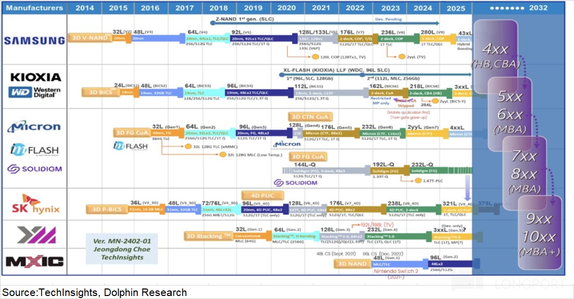
To compare NAND products, look at layer nodes, area density (Gb/mm²), architecture choices such as CBA bonding or cell type, and interface and R/W performance. These define the competitive curve.
Iteration pathways include higher stack counts, higher bit density, architectural and process advances, and bits-per-cell choices. Sandisk chose not to fixate on layer counts, instead prioritizing lateral scaling, early CBA adoption, and HBF development to raise capacity per area by increasing pore density per layer.
a) Layer nodes
SK hynix currently leads in stacking. Its 321-layer QLC NAND SSD entered mass production and shipments in Apr 2026, the first 300+ layer QLC in volume and enabled by triple stack.
Others are close behind. At current mass nodes, the ranking is 321 (SK hynix) > 286 (Samsung) > 276 (Micron) > 218 (Sandisk/Kioxia), though gaps are narrowing.
Samsung’s V9 QLC (286 layers) saw volume delays due to design flaws but is now ramping after rework. The company converted legacy lines at Pyeongtaek P1 from Gen 6–8 to V9 and is expanding Pyeongtaek P4 PH1 and Xi’an, with V9 now over half of output.
In Aug 2026, Samsung debuted its 10th-gen BV-NAND (V10) with over 400 layers and later confirmed it will also switch to triple-stack for this product. The architecture shift is now industry-wide.
Micron’s G9 NAND (276 layers), launched in 2024, remains its shipping workhorse two years on. Micron has shifted focus to DRAM, slowing NAND progress, and the next gen (likely G10) is expected to volume in H2 2027.
Sandisk & Kioxia currently ship BiCS8 (218 layers), with BiCS10 (332 layers) sampling from Jul 2026 and BiCS11 in development. They co-use the same die design but differentiate via their own controllers and firmware.
b) Area density (Gb/mm²)
Despite fewer layers, Sandisk & Kioxia lead in area density. Their roadmap centers on boosting storage pore density and tighter cell packing to lift bits per wafer, rather than merely stacking more layers, which raises fab capex and process complexity.
BiCS emphasizes lateral micro-scaling. In practice, that means thinning layers and tightening pore pitch to fit more bits in the same area, reducing overhead area. The trade-off is higher risk of charge interference and potential wear and reliability challenges as layers thin.
Given this, Sandisk & Kioxia steer BiCS9 toward AI PCs and phones, and BiCS10 toward AI inference and enterprise. BiCS9 is a minor spin on BiCS8 with a modest layer bump (218 to ~230).
Exact area densities are undisclosed, but market estimates suggest: Sandisk & Kioxia BiCS10 (>29) > Samsung V9/V10 (28) > Micron G9 (21) > SK hynix Gen9 (20), all in Gb/mm².
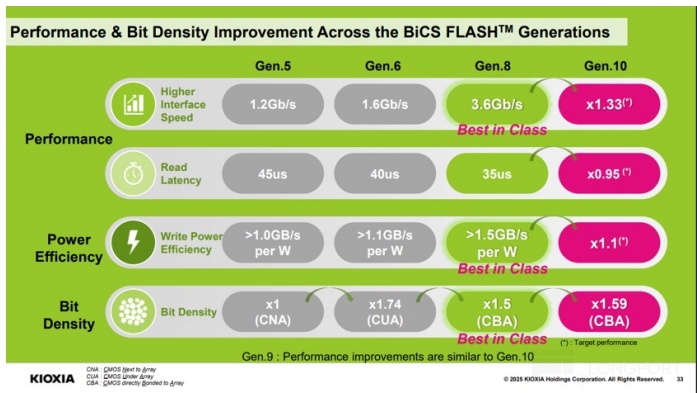
c) Architecture (CBA bonding / cell type)
CBA: Sandisk & Kioxia led on CBA, first mass-producing CMOS Bonded to Array in BiCS8 (2024). Logic and array wafers are built separately on optimal nodes, then Cu-Cu hybrid-bonded to deliver higher density, faster I/O, and smaller die, forming the basis for HBF.
Samsung and SK hynix began adopting CBA in 2026, while Micron has yet to deploy it and is expected to introduce it at 300+ layers. The direction of travel is clear across the industry.
CBA boosts efficiency by isolating control circuitry from high-temperature steps and freeing array area from control logic. Storage cells can be packed denser, and layer heights can be compressed further for better scaling.
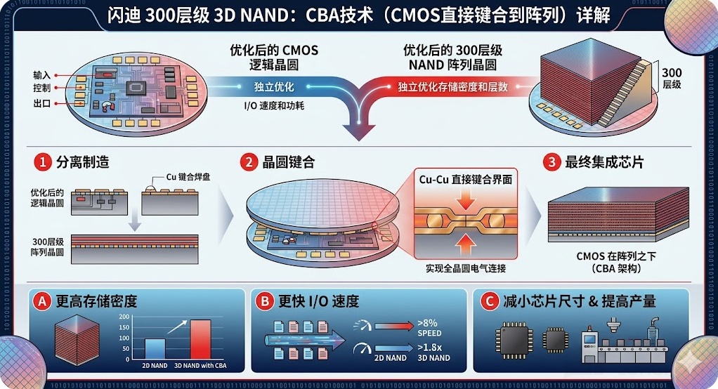
Cell types: QLC (4 bits/cell) is the mainstream for enterprise capacity. Sandisk’s BiCS8 supports 'UltraQLC' with a 2Tb large die, and SK hynix ships 321-layer QLC. Sandisk’s product strategy positions TLC (3 bits/cell) for performance and QLC for capacity with BiCS9 for 1Tb TLC die. It explicitly avoids PLC (5 bits/cell), leaning on CBA plus lateral scaling for better perf./efficiency.
TLC, QLC, and PLC refer to how many charge states a cell must hold. Going from TLC to QLC to PLC raises density but also increases wear and can shorten usable life, a key trade-off in enterprise use.
d) Interfaces and R/W performance (data rates)
Among vendors, current interface speeds are broadly similar. Mainstream products run 3.2–3.6Gbps, and next-gen parts are expected at 4.8–5.6Gbps, narrowing the gap.
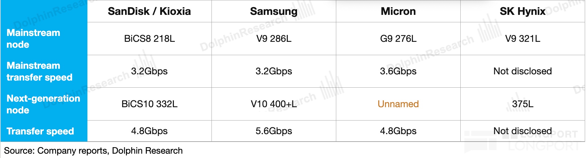
There are two interface camps: Toggle DDR and ONFI. Sandisk & Kioxia and Samsung use Toggle, while Micron and SK hynix use ONFI, with slightly different rate bins and roadmaps.
Samsung’s V9 remains on Toggle 5.1. Sandisk/Kioxia are more aggressive, already moving to CBA plus Toggle DDR 6.0 on BiCS9 for high-performance client and enterprise SSDs, including AI workloads.
HBF (High Bandwidth Flash) is the largest interface variable. SK hynix and Sandisk jointly unveiled the spec at FMS 2026, with 8-Hi and 16-Hi die stacks and capacity up to 512GB, targeting ~1.6TB/s bandwidth and microsecond-level latency, 8–16x HBM capacity, and performance between HBM and NVMe SSDs (7–14GB/s).
Traditionally, NAND sits behind an SSD controller and connects via PCIe to the CPU. HBM is fast because of short distance and wide interfaces, sitting adjacent to the GPU, and HBF brings that package-level interface to NAND, yielding HBM-class read bandwidth with 8–16x HBM capacity.
Note that HBF’s random read latency is around 10μs versus HBM’s 10–100ns, a 100–1000x delta. HBF will not replace HBM, but adds a new tier between HBM and SSDs, better for dense inference where weights and large context can be prefetched and throughput matters more than single-access latency.
Sandisk’s HBF progress: the first HBF die has taped out, with initial inference product samples expected in CY27. The roadmap is taking shape alongside partners.
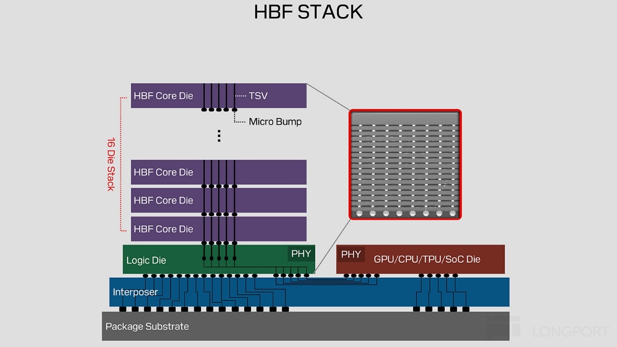
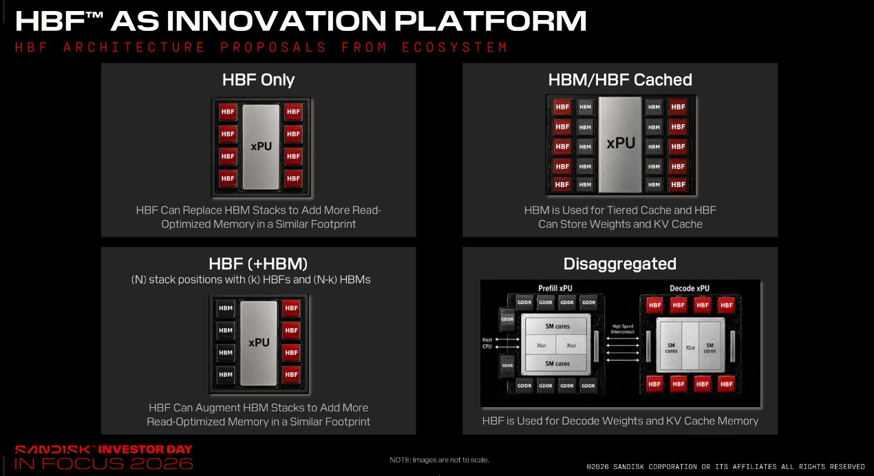
Sandisk’s four HBF deployment modes
1) Replacement: pure HBF. Replace all HBM stacks with HBF in the same package footprint, placing weights and KV cache entirely on HBF, maximizing capacity at the same bandwidth but with no HBM buffer and no write buffer, making it most sensitive to NAND endurance as every token’s KV writes hit NAND.
Note: programming and erase rely on high voltage to tunnel electrons through the oxide, leaving trap charges that accumulate and eventually degrade retention. This is the fundamental endurance limit.
2) Cached: HBM/HBF cached. HBM moves to the front-end as a low-latency cache, with weights and KV cache on HBF. This cuts HBF access frequency, but as long as KV lands on HBF, write constraints remain.
3) Augmented: HBF + HBM mix. HBF takes part of the stack positions around the XPU, with the rest staying HBM and tasks split. This is the lowest-barrier option, as accelerators need not abandon HBM to add HBF, and thus the most likely first-gen deployment with weights on HBF and KV cache on HBM.
4) Disaggregated. Move HBF off-package into a pool storing decode-stage weights and KV cache, with a smaller adjacent HBM cache. As HBF will likely not replace HBM wholesale, this could catalyze disaggregated inference architectures, a direction already backed by Google, Meta, SK hynix, and Tenstorrent within the HBF alliance.
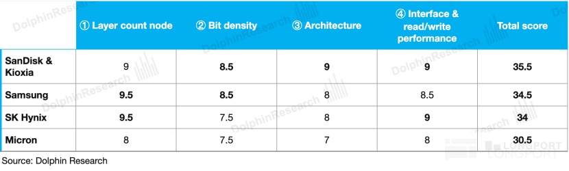
Across these four dimensions, Sandisk remains relatively ahead, notably in area density, CBA, and interfaces including HBF. While layer counts once lagged, BiCS10 brings it back into the first tier.
SK hynix and Samsung are now introducing CBA as well. Micron’s focus remains DRAM-heavy, and its NAND progress is comparatively slower in this cycle.
Dolphin Research focused here on Sandisk’s ties with Western Digital, its partnership with Kioxia, and the state of NAND technology. The next note will cover business progress and valuation; please follow for updates.
<End>
Related history on Sandisk by Dolphin Research:
Aug 17, 2026 Hot Take: Is Sandisk an even bigger cash cow than DRAM?
Aug 14, 2026 Trans: Sandisk (Minutes): $90bn contracts, 80% GPM, 50% Adj. FCF margin, all going to shareholders!
Risk disclosure and disclaimer: Dolphin Research disclaimer and general disclosure


The copyright of this article belongs to the original author/organization.
The views expressed herein are solely those of the author and do not reflect the stance of the platform. The content is intended for investment reference purposes only and shall not be considered as investment advice. Please contact us if you have any questions or suggestions regarding the content services provided by the platform.