

NVDU
----
D
5 hours ago
存力接棒算力,HBM 為什麼 “脱穎而出”?
 I'm LongbridgeAI, I can summarize articles.
Looking back from today at H2 2025, this marked a pivotal inflection for the AI hardware supply chain. Until then, 'compute' led by NVIDIA GPUs sat center stage. After that point, 'memory capacity' — spanning DRAM, NAND, and HDD — took over as the key bottleneck across the stack.
As the chart shows, DDR5 pricing surged roughly 7–9x in the six months after Sep 2025, while NAND prices climbed about 4–5x over the same period. In tandem, shares of Micron and SK hynix, the two DRAM leaders, spiked as much as ~10x within just half a year.
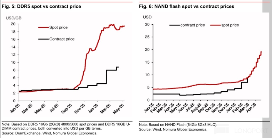
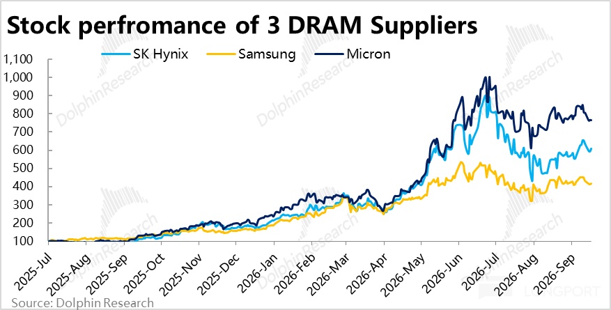
Dolphin Research has finally completed a review of this powerful memory upcycle and outlined a forward view in a themed series. Earlier, we used SanDisk as a case study to explore NAND fundamentals (cf. link).
Here, we begin with high-performance HBM, a scarcer segment. As the opening note, we take a bottom-up technical look and address three questions. We discuss the surge in AI memory demand, why HBM has become the default for leading GPUs, and the challenges and trade-offs behind HBM.
1) Why did AI memory demand seemingly explode in the past year, and what are LLMs’ core memory requirements? 2) Why did HBM — high-bandwidth memory — emerge as the preferred spec for top-tier GPUs, and what enables it to stand out? 3) What are the challenges and costs of HBM’s enabling technologies, and how might they reshape the memory value chain and vendors?
We build this foundation to support follow-on pieces on technology roadmaps, vendor differences, and the implications for the investment case. This will set up a deeper discussion of industry evolution and positioning.
Below is the main text:
I. Why has 'memory capacity' become the biggest bottleneck?
As AI advances, demand for DRAM/NAND has exploded to the point where memory capacity is often a bigger bottleneck than compute. Why did AI’s need for memory capacity and bandwidth spike seemingly overnight? The answer has two angles: much larger capacity and much faster data movement.
1.1 More capacity
In short, higher capacity needs stem from three factors: larger model parameters, bigger context windows, and Agent-driven workflows. These combine to push memory footprints sharply higher.
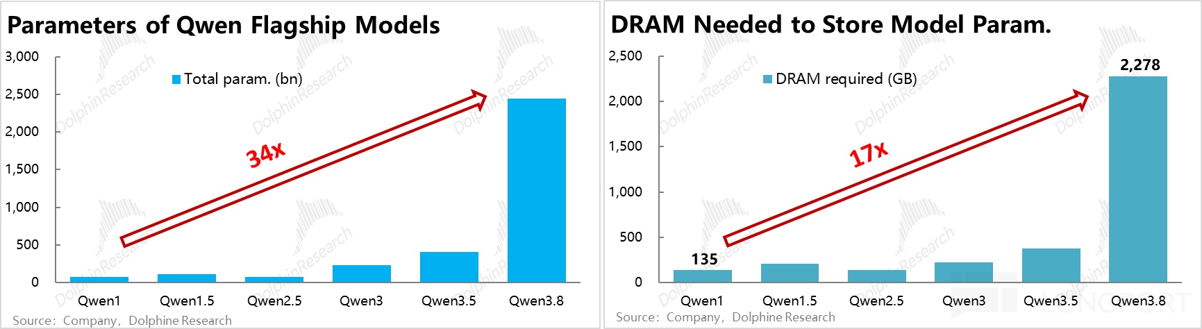
a. Parameters: The first memory block stores all model parameters. This scales almost linearly with the parameter count and the bytes used per parameter. Total memory depends on total params and precision per param.
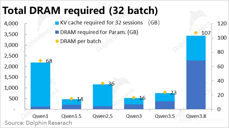
Flagship model sizes have risen by orders of magnitude over the past 3–4 years. Taking Qwen as an example, total params grew from 72 bn in the first-gen model to about 2.4 tn in Qwen 3.8 Max. That lifted per-instance parameter memory from 135 GB to nearly 2,300 GB — roughly 17x, even as precision dropped from BF16 (~2 bytes/param) to FP8 or lower (~1 byte/param).
(Earlier large models typically used BF16 at ~2 bytes/param, while recent storage precision is often FP8 or lower at ~1 byte or less.) This shift also helped temper the memory footprint per parameter.
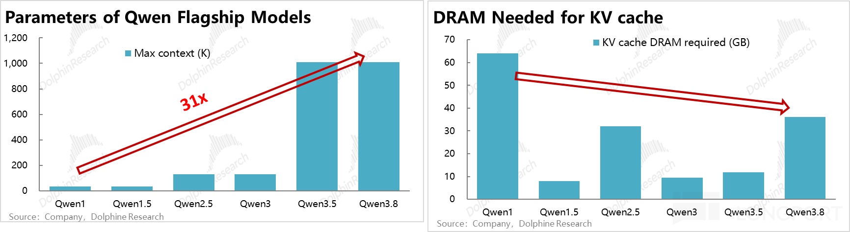
b. KV cache: Beyond fixed parameter storage, the elastic driver is the KV cache used in inference. This depends on context length and the model’s attention design and cache compression efficiency. It does not scale linearly.
From the first Qwen to Qwen 3.8 Max, context length expanded by about 31x, similar to parameter growth. However, due to cache innovation, memory growth for the cache rose far less.
By our estimates, Qwen 3.8 Max’s max context is ~8x Qwen 2.5’s, yet cache per session is ~36 GB, only ~12% above Qwen 2.5. These calculations assume 80% of max context utilization.
Even so, with rapid growth in users and sessions, aggregate KV cache can still expand by tens to 100x. Concurrency magnifies total memory needs.
For 32 concurrent sessions (at 80% of max context), a Qwen 3.8 Max instance requires roughly 3.6 TB in total memory. That breaks down to about 2.3 TB for parameters plus ~1.3 TB for KV cache.
c. Beyond LLM/Agent needs, Agent tasks create traditional compute and ops such as document writing or Excel operations. These also drive DRAM/NAND demand, though not necessarily at HBM specs.
1.2 Higher bandwidth
Capacity is one side; bandwidth is often even more critical in AI workloads. Two dynamics matter: keeping pace with faster compute to avoid starving the chip, and the explosive read/write demand from larger models and longer contexts.
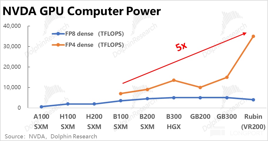
a. Faster chips need faster memory: For NVIDIA’s lineup, compute has jumped ~5x from B100 to VR200 (FP4 dense). Logically, memory bandwidth must rise in step to prevent underutilization.
For example, if a chip can process 1 GB/s but memory feeds only 0.5 GB/s, the GPU idles about half the time waiting on memory. This wastes compute.
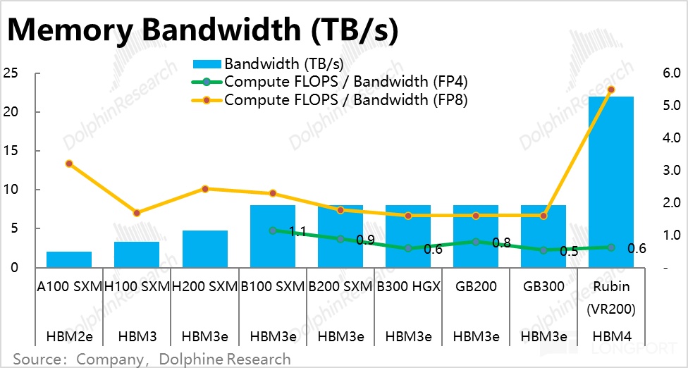
In practice, from B100 to GB300, five GPU generations held memory bandwidth flat at 8 TB/s (HBM3e). Bandwidth-to-compute declined from 1.1 to 0.5 on FP4.
VR200 raises bandwidth to 22 TB/s with HBM4, but compute also rises 2–3x, leaving the bandwidth-to-compute ratio at ~0.6. Memory bandwidth remains a relative bottleneck in the system.
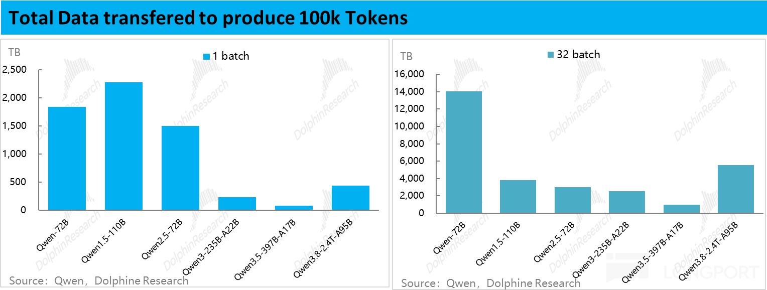
b. Quadratic growth in inference: Another driver is that inference reads scale roughly with the square of generated tokens, not linearly. Roughly speaking, 10x more context can require ~100x more data movement.
Each new token requires reading the full set of active parameters plus the entire prior KV cache. Generating n tokens repeats this read n times. This is a classic arithmetic series.
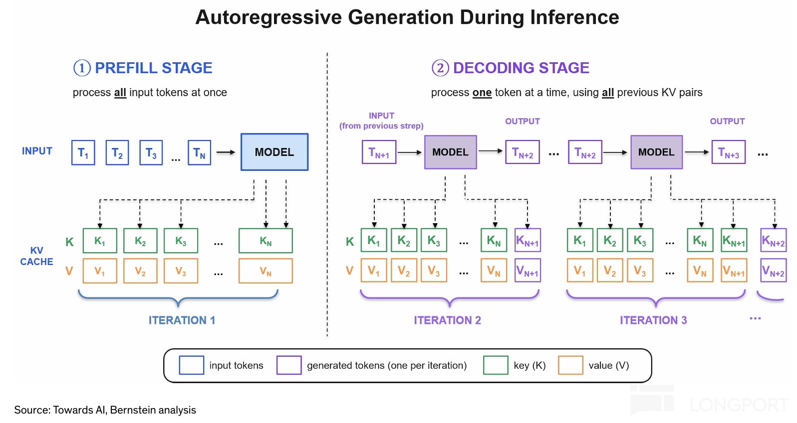
For Qwen 3.8 Max, starting with 100k context and generating another 100k tokens, total reads are on the order of ~500 TB. This highlights the scale of bandwidth pressure.
Even so, Qwen 3’s read/write needs are lower vs. prior models despite much larger params. Software advances are easing hardware requirements.
Two key shifts help: architectures moving from dense to sparse activation, and attention evolving from full to mixed/linear attention. These selectively compress or prioritize KV usage.
Yet, per the 'Jevons paradox', software gains free up hardware headroom that new models then consume with larger params and longer contexts — into the trillions or even tens of trillions. So read/write volume and bandwidth demands remain intense, even with efficiency gains.
And this view is per-model/per-session. With Agents and coding use cases, user and session counts are surging. With both per-user usage and user counts rising, total memory demand naturally multiplies.
II. Why did HBM stand out?
AI needs higher capacity and higher bandwidth. How does HBM deliver both and become the dominant memory for high-performance GPUs? Technically, HBM’s DRAM cells are similar to DDR; the core differences lie in architecture and packaging.
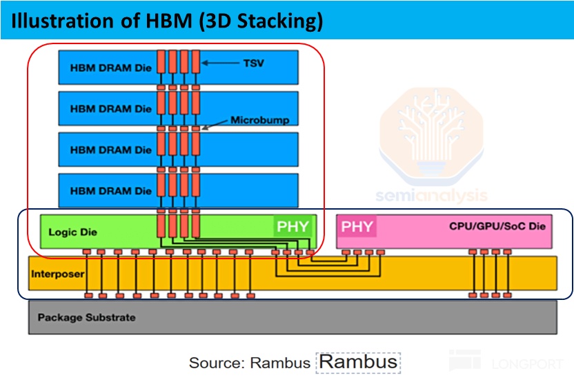
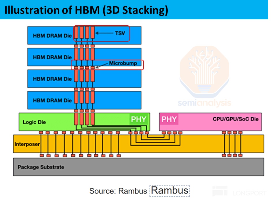
The diagram shows two signature HBM features: DRAM dies are vertically stacked, and HBM sits with the GPU on the same silicon interposer in a common package. These two innovations jointly enable high capacity and high bandwidth.
Key components include: ① DRAM dies, the actual memory cells; ② a logic/base die beneath the stack; ③ through-silicon vias (TSVs) for cross-die links; and ④ a silicon interposer that mounts and connects HBM and the GPU. We detail each component below.
2.1 Stacking boosts capacity
There are two ways to increase total capacity: raise per-die density, or pack more dies into the same footprint. In practice, both paths are constrained by physics and manufacturability.
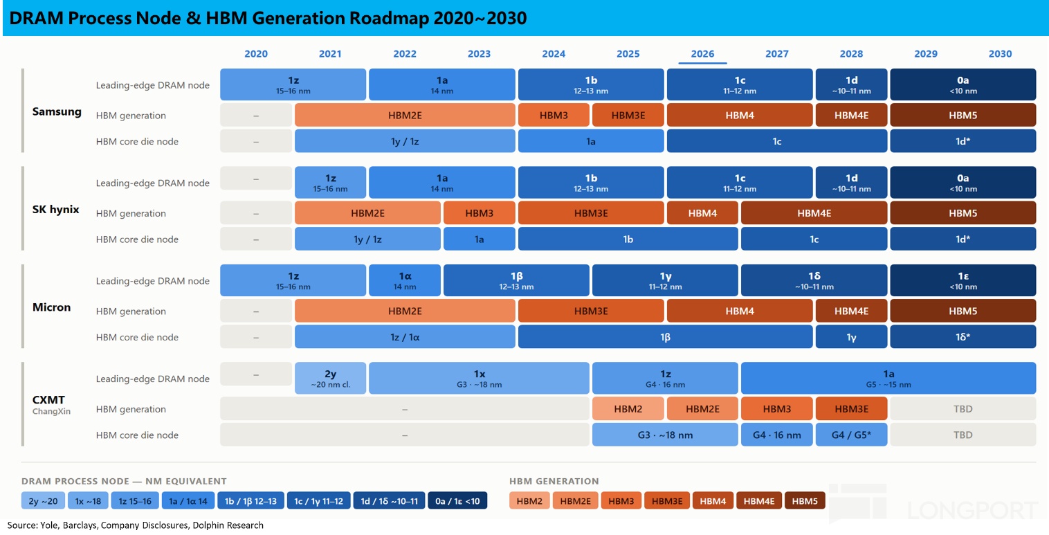
Die density hinges on process nodes, but DRAM scaling is hard. Nodes that are too small allow electrons to leak, causing data corruption. Today’s leading DRAM is ~11–12 nm, likely ~10 nm by 2030, far behind logic at 2–3 nm.
Unlike logic’s Moore’s Law, DRAM density gains via process shrink are limited. So the more feasible path is to stack more dies vertically in the same area.
HBM uses vertical stacking to increase capacity without expanding area. Under HBM4, stacks now reach 12 layers, 3x the first generation. Reports suggest the next wave, around 2026–27, may push to 16 layers.
2.2 Scarce area and edge constraints
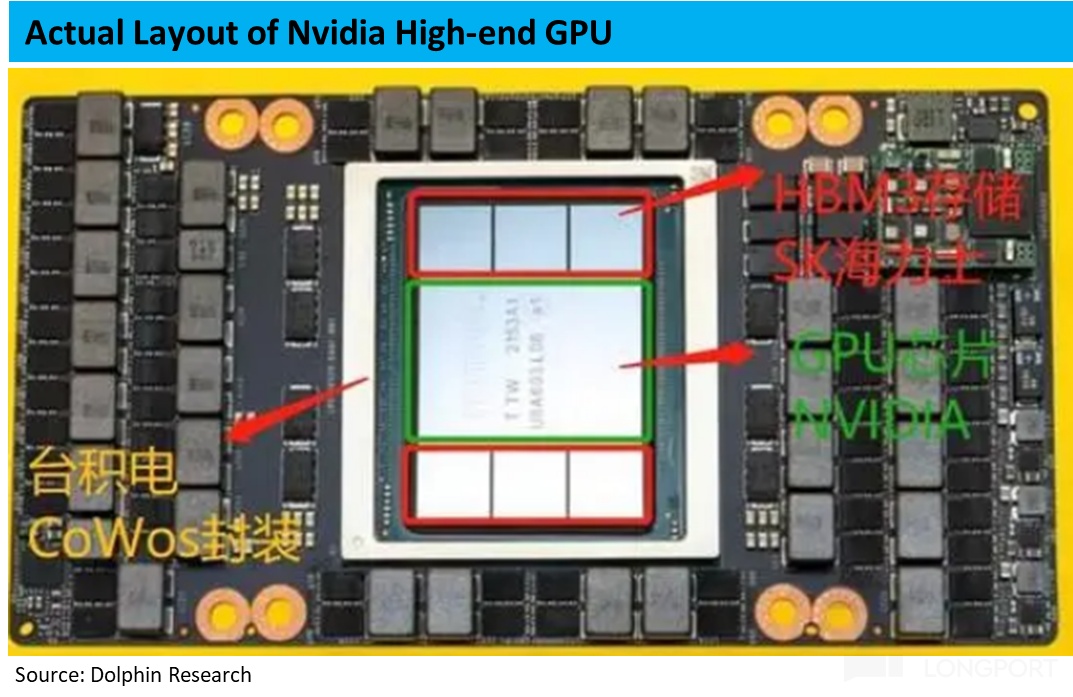
Why not place many dies flat on the substrate, as with traditional layouts, to reach higher capacity? Because high-performance GPUs have very limited real estate for memory.
To maximize bandwidth, HBM must be co-packaged close to the compute die on a dedicated silicon interposer. This severely limits where memory can be mounted.
a. As the photos show, consumer GPUs place the compute core in the metallic area, with GDDR chips around it on the black PCB. Server GPUs mount HBM right next to the GPU core within the metallic zone, which is area-constrained and cannot be expanded much today.
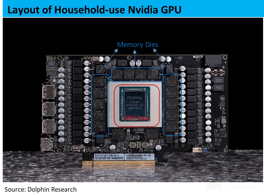
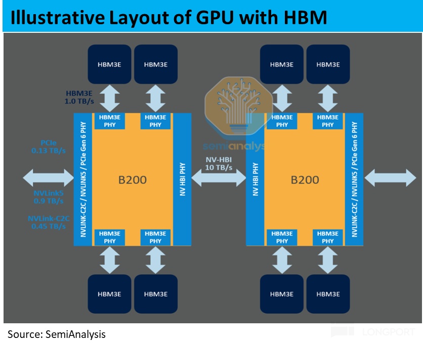
b. HBM stacks appear only above and below the GPU, with left/right edges left open. I/O must be routed along the four edges of the compute die.
Those edges also house on-die interconnects and external links, further squeezing memory placement. This limits lateral placement and necessitates vertical stacking.
III. HBM’s technical challenges
HBM brings clear benefits, but at a cost. We outline the main challenges.
3.1 Stacking difficulties
a. TSVs
Stacking raises the question of how to link dies for signals and power. The answer is TSVs — through-silicon vias. These are vertical holes in silicon filled with copper, enabling vertical communication and power delivery.
Each die face has micro-bumps aligned to TSVs, with spacing to prevent shorts and to aid thermal paths. TSV fabrication is mature across DRAM makers, but adds steps, cost, and yield risk.
TSVs must serve signaling, power, and thermal roles, so layout choices and yields help distinguish vendors. Design trade-offs here are key competitive factors.
b. Different bonding flows
TSVs and micro-bumps enable vertical links, but robust bonding and encapsulation are critical for long-term reliability. SK hynix uses MR-MUF (mass reflow plus a mold-underfill resin), while Samsung/Micron use TC-NCF (thermo-compression with a non-conductive film).
TC-NCF flow: apply a solid NCF to the lower die, align the next die, then heat/press so micro-bumps pierce the film and bond. The film melts, fills gaps, insulates, and sets on cooling. Repeat layer by layer until the stack is complete.
MR-MUF flow: align all dies at once with flux for temporary fixation, place the stack in a reflow oven to melt micro-bumps simultaneously, then inject a specialized liquid resin (EMC) to fill gaps and encapsulate. Cure and grind off excess resin.
MR-MUF tends to offer higher throughput, better yields, and improved thermals, translating into higher margins. This is a key competitive edge for SK hynix.
Reasons include fewer steps and single-pass reflow vs. multi-pass thermo-compression, plus reduced risk of wafer bowing, cracking, or bump damage under repeated heat/pressure. These factors improve yield.
Why not copy MR? SK hynix holds multiple patents, and the key resin is co-developed with upstream partners, limiting rivals’ access. Samsung and Micron have also invested heavily in TC tools and flows, making switching costly.
Rather than replicate MR, Samsung and Micron are pursuing next-gen hybrid bonding as a potential leapfrog path. Bonding technology choices are another axis of differentiation we will revisit.
3.2 Co-packaging
To increase bandwidth, HBM must be co-packaged with the GPU, which imposes tight area limits. Why does this architecture matter?
Bandwidth equals frequency times bus width. Bus width is the number of parallel lanes between memory and compute, while frequency is per-lane speed. HBM’s edge vs. GDDR is width, not per-lane speed.
HBM runs 1–2k-bit interfaces vs. 32-bit for GDDR. Per-lane efficiency is actually lower for HBM.
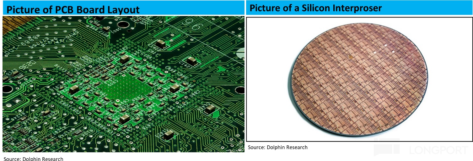
Routing thousands of ultra-dense lanes between memory and compute without crosstalk requires extremely narrow traces. PCB etching cannot meet this precision; only semiconductor processes can. Hence the silicon interposer.
PCBs typically support ~50 µm traces (visible to the eye), while silicon interposers can reach ~1 µm linewidths. This is the fundamental reason to add a silicon interposer to mount and connect HBM and the GPU.
3.3 Customized base dies
Similar to the interposer, the base die at the bottom of the stack increasingly relies on external foundries and co-design starting with HBM4. It serves as the hub: linking up to the stack and down through the interposer to the XPU for data and power.
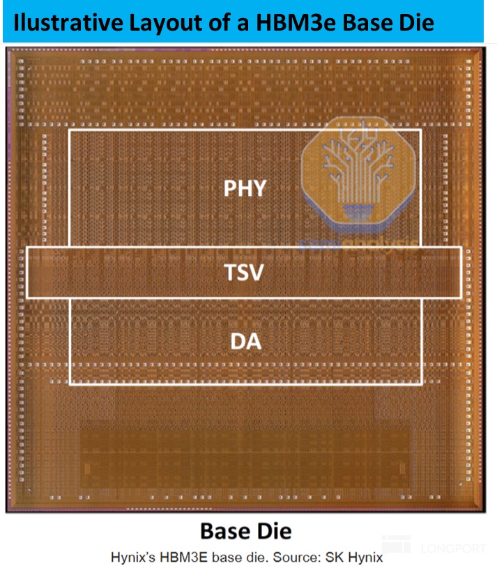
a. In HBM3e and earlier, the base die was simple, with three blocks: a PHY for XPU links, TSV blocks to the stack, and a Direct Access (DA) module for pre-package testing. At ~20 nm-class nodes, DRAM vendors could design and fabricate it in-house.
b. In HBM4, base-die nodes generally move to ~12 nm, and flagship variants will even adopt 2/3 nm at foundries like TSMC (Samsung can self-fab). This upgrade is driven by higher complexity.
HBM4 doubles interface width from 1k to 2k bits, requiring finer PHYs or much larger area, which is impractical. More importantly, memory controllers and address-mapping units are being moved from the XPU onto the base die.
This places control logic closer to memory, reducing round-trips between memory and XPU and freeing precious XPU die area. It also opens the door to more tailored memory subsystems.
c. Beyond process shrink, base dies are shifting from general-purpose to customer-specific designs. For example, NVIDIA’s NVHBM adopts a proprietary die-to-die protocol vs. JEDEC.
NVIDIA cites ~30% higher bandwidth, ~15% lower power, and ~25% area savings for compute. Marvell and Rambus have also announced customized base-die solutions.
3.4 Memory is no longer just for 'memory vendors'
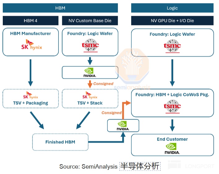
Co-packaging and customized, foundry-made base dies have two implications for HBM supply. First, DRAM vendors’ HBM output is constrained by partner capacity in base-die and advanced packaging (notably TSMC’s CoWoS), not just their own fabs.
In other words, high-performance memory is now a shared product among DRAM makers, OSAT/foundries, and end customers. Second, HBM specs and designs are increasingly co-developed with downstream customers, driving more customization.
Deep alignment with anchor customers becomes critical. Losing a lead account could strand bespoke designs. For SK hynix’s HBM4, the dies are made and stacked in-house, but the base die is co-designed with NVIDIA and fabbed at TSMC, with final packaging also at TSMC.
From this lens, DRAM vendors’ autonomy declines and their value capture may trend lower as the chain evolves. However, AI-driven growth has expanded the total value pool for HBM-class memory, so all participants are still benefiting.
IV. Closing
Across both demand and technology, the two core levers for memory are capacity/density and bandwidth. Today’s differentiation centers on stacking and packaging choices.
In the next piece, Dolphin Research will discuss how newer memory will trade off capacity, speed, and cost, and how those shifts may reshape the industry and vendors’ positioning. Stay tuned.
<End of full text>
Risk disclosures and statements: Dolphin Research Disclaimer and General Disclosures


The copyright of this article belongs to the original author/organization.
The views expressed herein are solely those of the author and do not reflect the stance of the platform. The content is intended for investment reference purposes only and shall not be considered as investment advice. Please contact us if you have any questions or suggestions regarding the content services provided by the platform.