

SNDQ
10.8101.91%
D
1 day ago, 05:25 AM
From HBM stack caps to a NAND ramp, NVDA vs. memory makers: who has the leverage?
 I'm LongbridgeAI, I can summarize articles.
In the prior piece, Dolphin Research started from first principles to explain why AI’s demand for memory capacity and bandwidth has 'suddenly' exploded, why HBM has become the default memory for high‑performance GPUs, and outlined the core concepts and logic behind HBM. As AI advances, the question is how memory technology will evolve to deliver larger capacity and higher bandwidth.
Coincidentally, two seemingly conflicting signals have emerged. On one hand, the HBM roadmap keeps pushing up stack heights from 12 layers to 16 and 20. On the other, per SemiAnalysis, the HBM in NVIDIA’s next‑gen Rubin Ultra may cut from 16 layers to 8, while HBF, a flash‑based alternative, is vying to take a slice of capacity from HBM.
Will HBM be displaced or become even scarcer. Should HBM keep stacking higher. Following the three threads of capacity, bandwidth, and cost left in the last article, this piece discusses:
1) What paths can the industry take to keep expanding memory capacity, and at what cost. Why might HBM layers not rise but fall.2) Why bandwidth is harder to scale than capacity, where the bottlenecks lie, and what breakthroughs are in sight.3) Which routes are more likely by workload, and how they could reshape the value capture across the chain and memory makers’ bargaining power.
What follows is the main text:
I. How to expand capacity
Start with capacity scaling. The industry is pursuing two parallel approaches: one is to push process limits and make a single memory die stronger, at the cost of more complex processing, higher cost, and potentially lower yield; the other favors cost‑performance, forgoing peak per‑die specs and winning by volume, matching different SKUs to tiered needs. Both routes trade off cost, yield, and performance.
1.1 Path 1: Stronger per‑die performance
a. Keep stacking more layers
The most direct way is to keep adding layers along the current path. HBM3E is 12‑high, some HBM4/4E will reach 16‑high, and the HBM5 roadmap points to 20‑high. But stacking more is not as simple as it sounds.
Because HBM and the XPU are co‑packaged, sharing the same base and lid, the total stack height is capped. The spec limit was 720 µm up to HBM3E and relaxed to 775 µm in HBM4. This constrains how much you can stack.
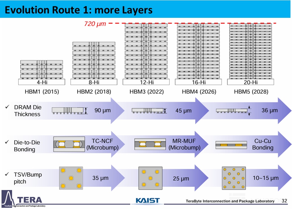
Under a height limit, you have two options: (i) thin each DRAM die; (ii) shrink inter‑die spacing by using smaller micro‑bumps or even removing them altogether and switching to Cu‑Cu bonding for direct copper‑to‑copper contacts. Both drive tighter tolerances.
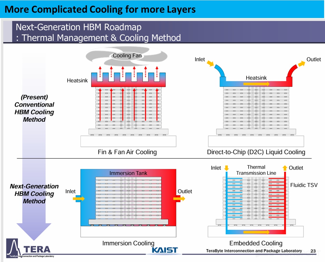
Finer processes mean higher cost and lower yield. Thinner wafers lose mechanical strength, increasing warpage and damage risk during stacking; reduced spacing makes thermal management and dielectric fill harder, and TC‑NCF gives way to SK Hynix’s MR‑MUF or hybrid bonding; more layers raise power delivery, signaling, and thermal requirements, forcing denser, narrower TSVs. In short, you buy incremental capacity with tougher processing and higher cost, and ask more of memory makers. The upside is every added GB sits on the front‑row HBM and enjoys peak bandwidth.
b. A shortcut around the height cap
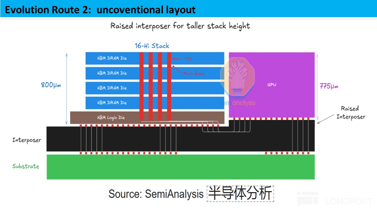
A 'shortcut' is to effectively increase stack headroom. As shown below, raise the interposer under the GPU so the GPU and HBM still sit level on top, but the HBM stack gains usable height to roughly 800 µm. This reduces or avoids die thinning while adding a few layers, saving cost and yield loss from more complex processes.
The extra headroom is limited. Going from 720 µm to ~800 µm, with only slightly narrower per‑layer pitch than 45 µm, you can at most add two layers. So the benefit tops out quickly.
1.2 Path 2: Win by quantity
a. Multi‑row memory: speed up front, capacity in back
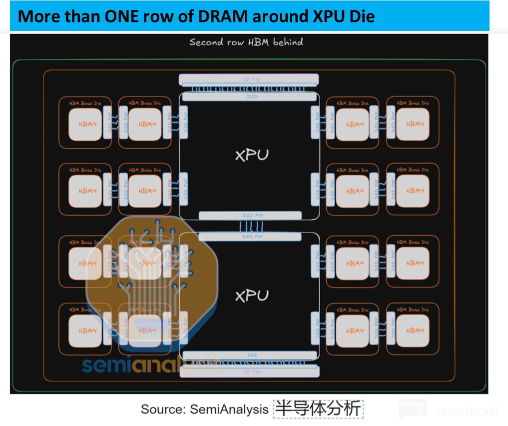
The other path is to add more memory stacks. Because space near the XPU is scarce, additional memory will likely sit in a back row, which avoids ultra‑dense stacking processes but inevitably offers lower bandwidth. That is the trade‑off.
You have choices in memory type and packaging. Spec‑wise, the back row could use HBM as shown, or switch to standard DDR, or even HBF (discussed later) based on NAND for lower $/GB; packaging‑wise, the back row can sit with the XPU on the silicon interposer for higher speed but higher cost and limited interposer area, or on a substrate or even the PCB for lower speed but cheaper and with ample area. Designs will vary by target workload and budget.
But you cannot add back rows without bound because bandwidth becomes the bottleneck. Data from the back row must traverse the front row, so the aggregate is capped by the bandwidth between the front‑row HBM and the XPU. For instance, if HBM‑to‑XPU bandwidth is 4 TB/s and 2 TB/s is consumed by the front row and XPU traffic, only 2 TB/s is left for back‑row relay, and a third row would squeeze it further. That is a hard ceiling.
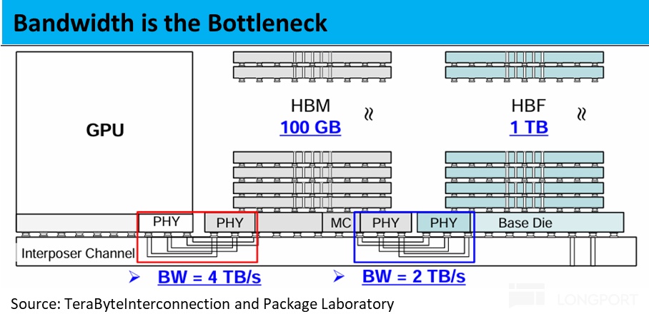
b. HBF: a cheaper option
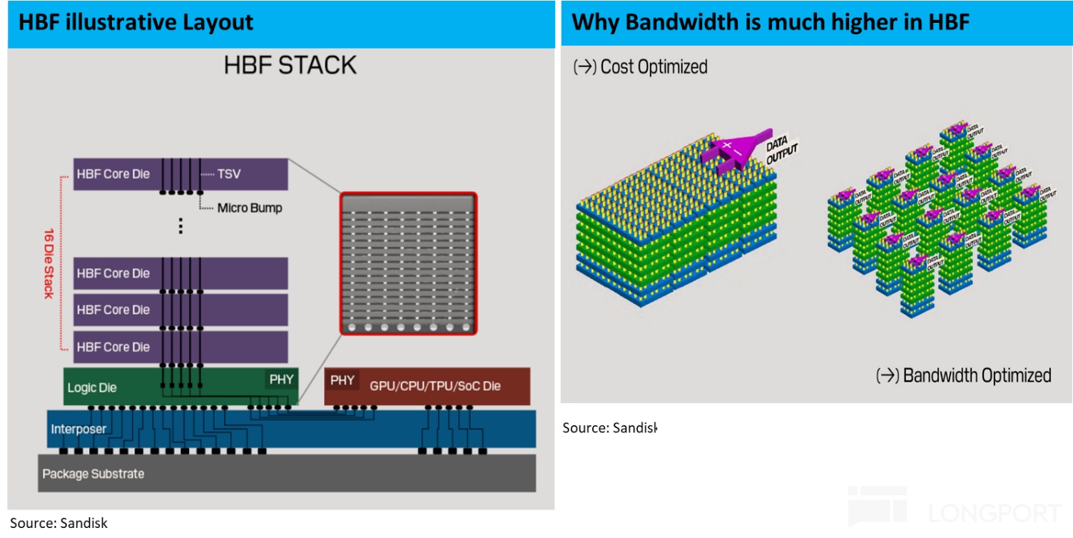
To cut $/GB, the industry is evaluating memories other than HBM, and one major candidate is HBF, or high bandwidth flash. As the name suggests, its structure largely mirrors HBM with a multi‑die stack, TSVs to connect dies, and co‑packaging with the XPU, except that DRAM dies are replaced with NAND. It aims to mix capacity with reasonable bandwidth.
A natural question is why HBF needs multi‑die stacking given NAND is already 3D. The reason is NAND’s '3D' stacks storage layers, which adds capacity but not more readout channels, since cells in a string share a read path and only one layer can be read at a time. The HBF bandwidth bump comes from parallelism.
Each die is partitioned into many small arrays read in parallel, and 16 dies are stacked with TSVs to output concurrently. Conventional 3D NAND also stacks capacity but shares one bus and transmits in turn, as detailed in Dolphin Research’s NAND report. This architectural difference is key.
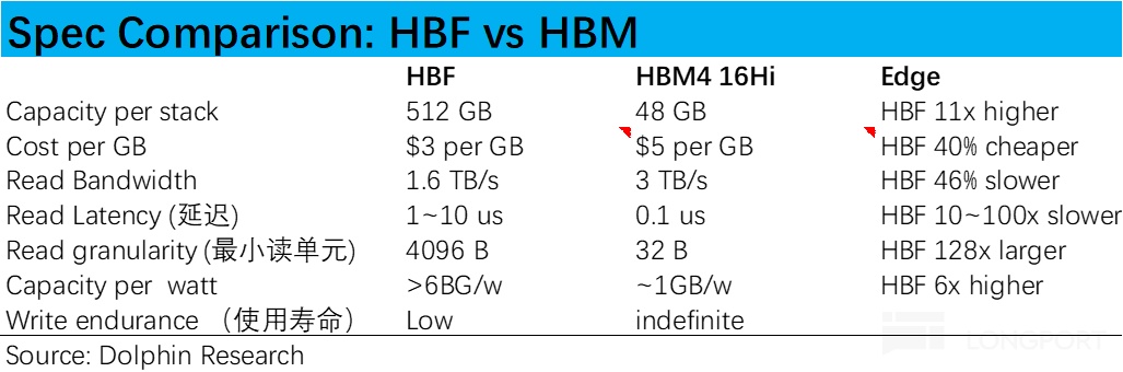
HBF’s pros and cons vs. HBM are clear. First, it is big, cheap, and power‑efficient: HBF Gen1 (16‑high), expected around late 2026 to early 2027, targets 512 GB per stack, while a 16‑high HBM4 is 48 GB, and HBF’s $/GB could be roughly half of HBM per checks, with naturally lower power and thermal needs for NAND.
Second, it can reach the same order of magnitude in bandwidth. With similar stacking and co‑packaging, disclosed read bandwidth for HBF Gen1 is up to 1.6 TB/s (writes are much slower), about 55% of the HBM4 spec peak. That makes it viable for colder data.
Third, NAND’s inherent traits preclude replacing HBM: high latency, slow writes, block‑based reads, and limited P/E cycles. Read latency is ~1–10 µs vs. ~0.1 µs for DRAM, writes are 10–100x slower, and block reads bring extra data, reducing effective bandwidth. So HBF only fits data that are not frequently read or written.
As such, HBF suits full model weights (not activations), compressed context caches, and MoE expert weights not yet invoked. Workload placement matters.
c. Hybrid architectures: the likely outcome
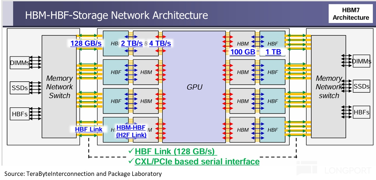
No single approach can maximize speed, capacity, and cost at once, so the most likely longer‑term answer is multi‑tier, hybrid memory. One side of the XPU package integrates HBM to handle high‑frequency traffic, while the other side integrates HBF to provide larger capacity for lower‑frequency data. This balances $/GB and bandwidth.
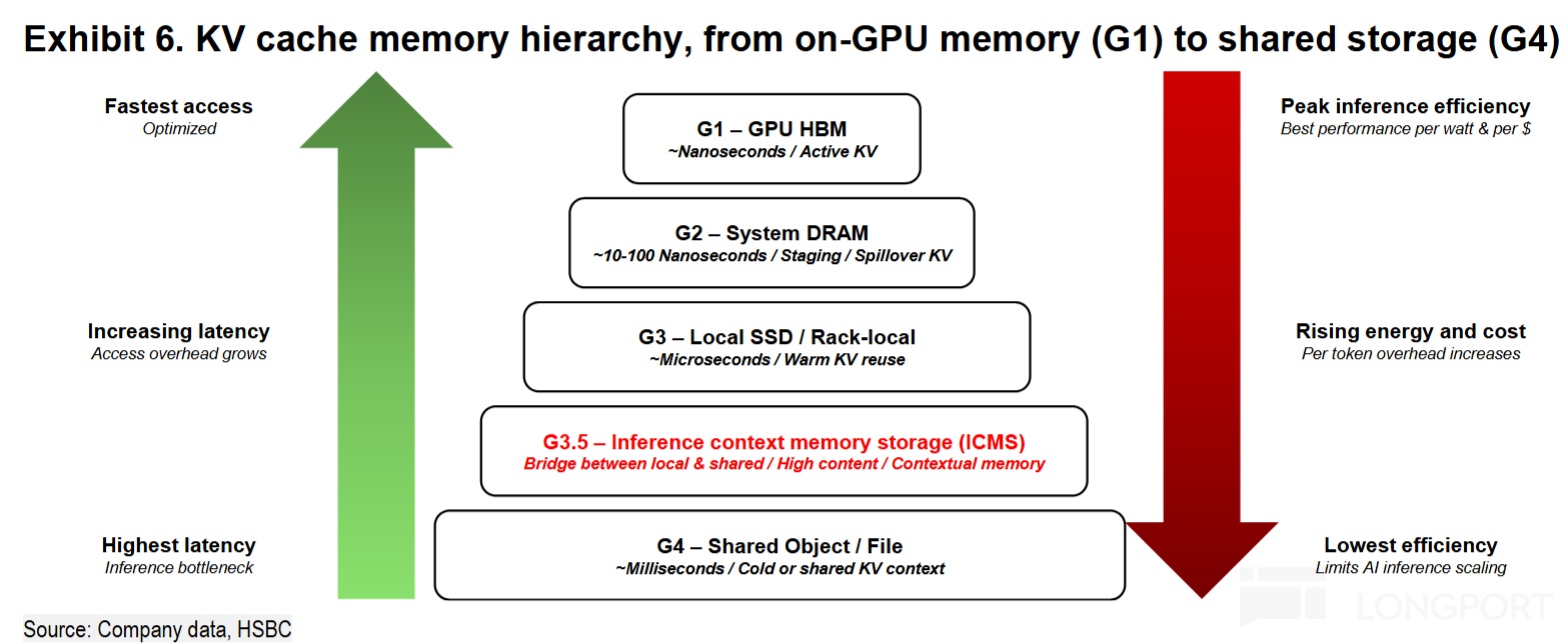
Further out, the HBM7 concept adds a pooled tier over PCIe so each XPU can access system‑wide DRAM, SSD, and HBF. Each tier serves a role: HBM holds hot parameters and KV cache, DDR and HBF serve secondary tiers, and pooled SSD‑class storage keeps colder data. This hierarchy optimizes both cost and performance.
1.3 Could HBM layers go down, not up
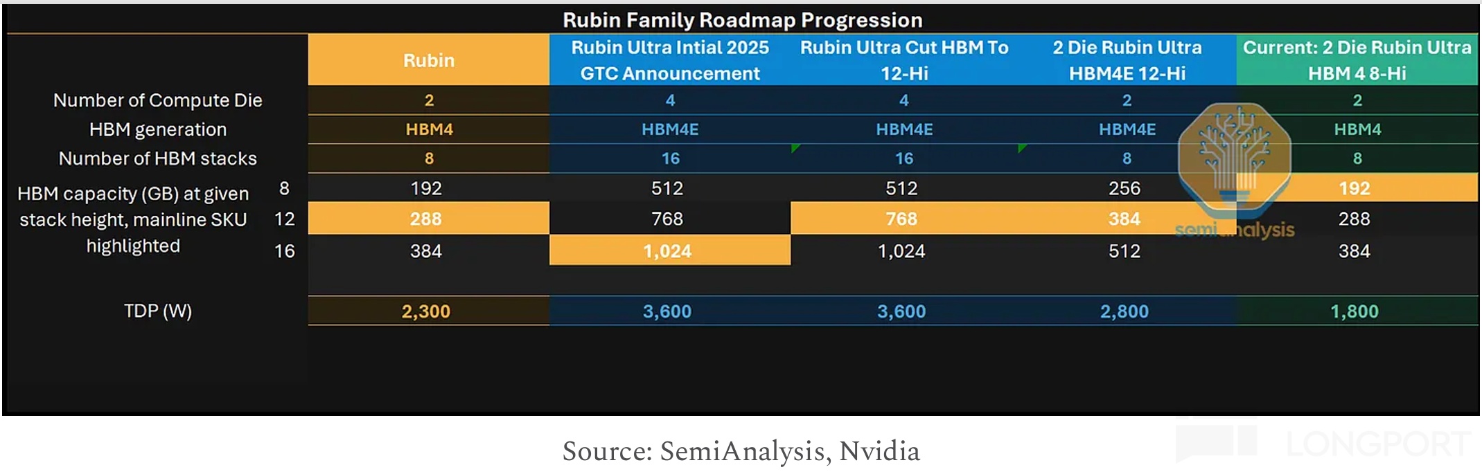
A hot topic lately is that HBM stack heights might not rise but fall. The trigger is NVIDIA’s Rubin Ultra, where each compute die pairs with four HBM stacks that reportedly moved from 16‑high to 12‑high and may shift to 8‑high per supply chain chatter. Total HBM capacity per GPU would fall from 768 GB to 192 GB.
Note these changes are unconfirmed by NVIDIA and only indicate options under consideration. But they do frame a plausible direction.
Beyond the difficulty and cost of taller stacks, three other factors may drive a shift to fewer layers. First, DRAM wafer capacity is limited.
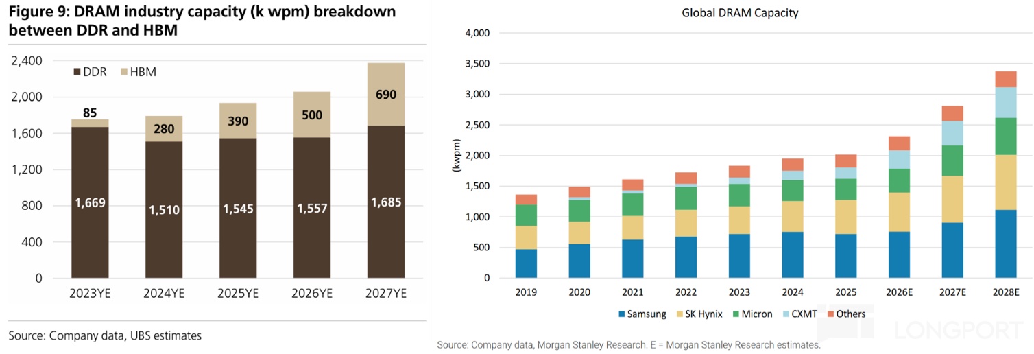
Producing the same GB output, HBM already consumes 3–4x the DRAM wafers vs. commodity DRAM. If layers go higher, DRAM wafer loss rises further, so total memory output falls for the same line count, and new DRAM capacity takes time, with forecasts showing only limited growth in 2024–26 and more release in 2027. This wafer cap is likely the main near‑term constraint on HBM stack heights.
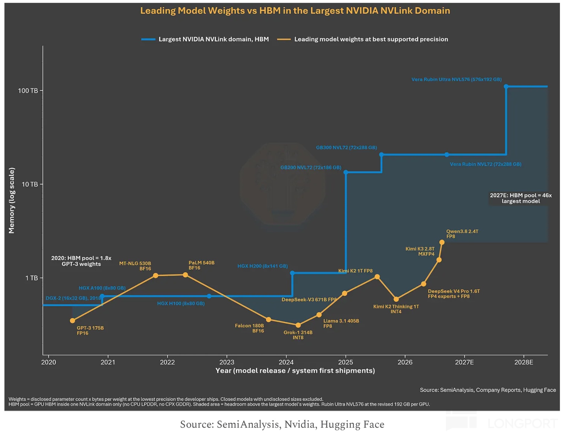
Second, larger scale‑up interconnects lift system capacity even if per‑GPU memory shrinks. With scale‑up inside a rack, GPUs per rack jump, boosting total pooled capacity. For example, B300 pairs eight 12‑high HBM3E stacks for 288 GB per GPU and scales to 72 GPUs per rack for ~20 TB total, whereas Rubin Ultra with eight 8‑high HBM stacks for 192 GB per GPU could scale to 576 GPUs, pooling ~110 TB.
Per‑GPU capacity falls by one‑third, yet system capacity is roughly five times higher. This shows a path to win by numbers under capacity constraints.
So reducing layers effectively lowers process risk and cost and wins by quantity under limited DRAM wafers. It is rational, but it introduces two new pressures. First, the bottleneck shifts to Base Die and co‑packaging capacity.
Using more low‑layer HBM saves DRAM wafers but consumes more co‑packaging capacity. The key moves from memory makers’ own expansion pace to how much capacity can be locked at TSMC, Samsung, or Intel. Second, it raises interconnect requirements.
Fewer layers demand more footprint, thus more co‑packaging slots, and the saved wafer output shifts to DRAM, while memory demand keeps rising. That naturally raises the bar for memory pooling. Pressure then moves to interconnect tech that boosts memory utilization.
a. HBM pooling under massive GPU scale‑up: Rubin Ultra, with fewer HBM layers, scales from 72 to 144 GPUs in‑rack and up to 576 across racks. Each GPU’s HBM connects at a shared address space to form a larger HBM pool for GPU compute and model parameters. This leverages scale to offset per‑GPU memory cuts.
b. DRAM pooling: Use CXL switch chips to pool commodity DRAM, much like NVLINK connects multiple GPUs, to form a large DRAM pool for long‑context and Agent workloads. Additionally, NVIDIA’s CMX product pools NAND for less frequently accessed context memory.
II. Packaging and bandwidth: two other key levers
The layer‑count debate highlights two variables: whether bandwidth can keep rising meaningfully, because stacking only helps if bandwidth scales, and whether co‑packaging and Base Die capacity are adequate, because fewer‑layers‑more‑stacks only works if capacity is available. This brings us to packaging and bandwidth.
2.1 CoWoS packaging
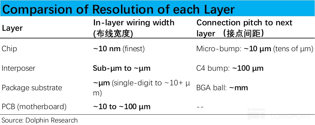
As noted earlier, HBM’s high bandwidth relies on co‑packaging with the XPU on a silicon interposer. This is centered on TSMC’s CoWoS (Chip‑on‑Wafer‑on‑Substrate), which stacks three levels: the top chips, the middle interposer wafer, and the bottom substrate. Its role is akin to a funnel that fans out nanometer‑scale wiring to millimeter‑scale board connections.
As shown, chips connect to the interposer via micro‑bumps, the interposer connects to the substrate via C4 bumps, and the substrate connects to the PCB via BGA balls, with alignment tolerance loosening at each level. That hierarchy underpins HBM‑class wiring density.
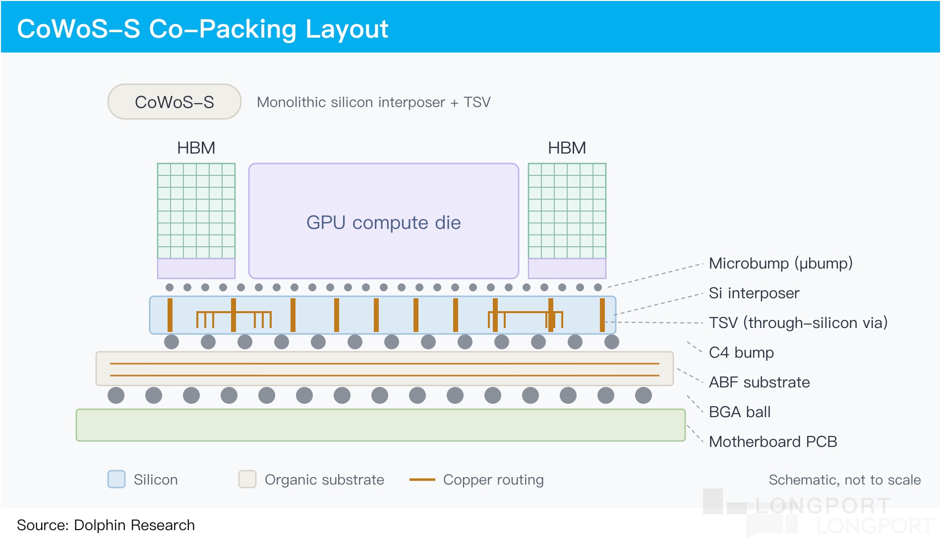
CoWoS has three variants differing in the interposer: S (silicon) uses a full silicon interposer; R (RDL) uses copper lines with dielectric layers like a PCB; and L (LSI, local silicon interconnect) combines the two. Each targets a different cost‑precision trade‑off.
CoWoS‑S is not just expensive but area‑limited. A full silicon interposer relies on a single lithography exposure of up to ~858 mm², and larger areas require stitching, which hurts yield, with today’s limit at roughly 3.3x a single exposure. That caps how large a monolithic interposer can be.
CoWoS‑R replaces the silicon interposer with an RDL stack made from copper, dielectrics, and encapsulation, akin to PCB processes. It is cheaper and can be larger without semiconductor tooling, but its routing precision is lower and unsuitable for HBM, so we will not dwell on it. It targets lower‑density use cases.
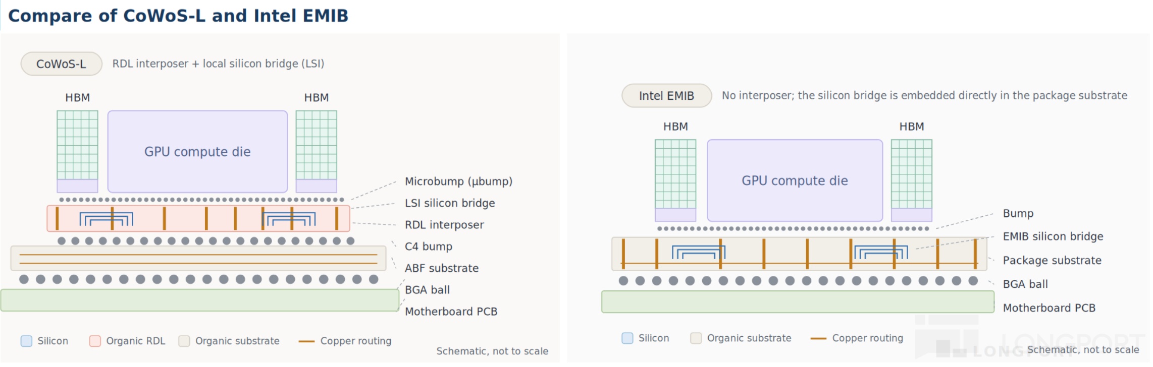
CoWoS‑L uses an RDL base and embeds small silicon bridges only where high precision is needed, such as at the HBM‑to‑XPU interface. With this, interposer area has reached ~5.5x a single exposure, and NVIDIA adopted it starting with the B200 series. This variant has become the mainstream.
Intel and Samsung have similar co‑packaging flows. Intel’s EMIB is even simpler with no full interposer, embedding silicon directly into the substrate at high‑precision junctions, though EMIB is mostly used for Intel’s own products, and external clients like TPUs and Trainium are reportedly still evaluating it. Options are broadening as customers diversify vendors.
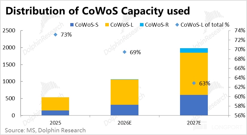
Broker models show CoWoS‑L above 60% share and rising. Compared with DRAM wafers, which see limited growth until 2027 when capacity steps up ~15–20%, CoWoS capacity is expanding faster, roughly doubling in 2027 vs. 2026. This supports the case for more, lower‑layer HBM stacks over fewer, taller stacks.
In short, CoWoS‑L and EMIB both cut packaging cost and raise the maximum assembly area, allowing a single GPU to host more memory stacks. This underpins the multi‑row memory concepts discussed earlier. Packaging thus becomes a central lever in system design.
2.2 Width vs. rate: can both rise at once, and how else to boost bandwidth
Per‑stack bandwidth equals bus width (number of parallel lanes) times data rate (speed per lane). A GPU’s total memory bandwidth equals per‑stack bandwidth times the number of stacks, and adding stacks is straightforward but limited by perimeter area around the XPU. So focus shifts to how to lift per‑stack bandwidth.
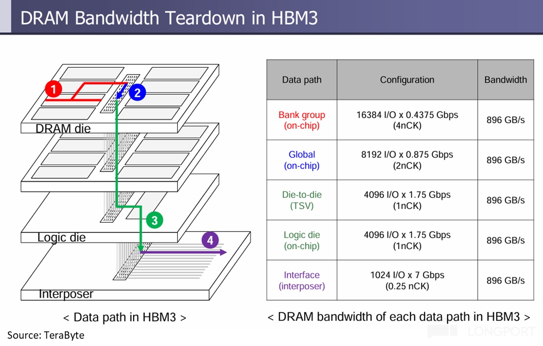
Per‑stack bandwidth comprises internal and external bandwidth. Internally, data flow from banks to each layer, and through TSVs up the stack to the Base Die; externally, the Base Die sends data across the interposer to the XPU. Both must accelerate to raise the total.
Today’s bottleneck lies more in external bandwidth, with difficulty concentrated in Base Die and interposer design and manufacturing. Internal paths are shorter and can be improved by adding TSV channels, which is feasible with a clear path forward. That is why Base Die and interposer tech are focal points.
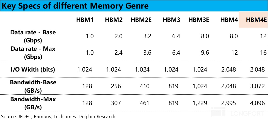
Bus width and data rate seem like allies but often compete. From HBM1 to HBM3E, width held at 1024 bits and bandwidth gains came almost entirely from higher rates, though rate gains are slowing from per‑gen doubles to 25–50% steps; when HBM4 doubled width, the initial standard rates plateaued around 8 TB/s, with later increases. It is hard to push both at once.
What limits width and rate, and why do they compete. Width equals the total routing area divided by line pitch (line width plus spacing), so raising width requires narrower lines and spacing via higher‑precision etch, or more interposer area devoted to routing, alongside larger PHY areas on the HBM Base Die and XPU. Area and precision are the core constraints.
Rate is bits per second per line, akin to water speed in a pipe, which rises with higher source drive (frequency and voltage) and shorter, thicker lines with wider spacing to cut crosstalk. Base Die must drive faster at higher power and thermal load, one reason it is fabricated on advanced nodes by TSMC and others. The conflict is that width wants finer, dense lines while rate wants thicker, spaced lines on the same finite area.
Thus, to keep pushing bandwidth, there are three main levers. Improve Base Die design and process to transmit faster and cleaner signals; enhance interposers with better shielding and more routing layers; and shorten line lengths via 3D stacking by placing HBM above or below the XPU, where width and rate do not conflict on length. These define the roadmap for bandwidth scaling.
III. Stronger per‑die or win by numbers: where is the pivot
We have outlined capacity and bandwidth paths. Capacity has multiple routes that essentially balance cost, capacity, and bandwidth, while bandwidth gains converge on Base Die, interposers, and packaging. The next question is whether the industry prioritizes capacity or bandwidth, and how that shifts value to memory makers.
3.1 How much pricier is HBM vs. others
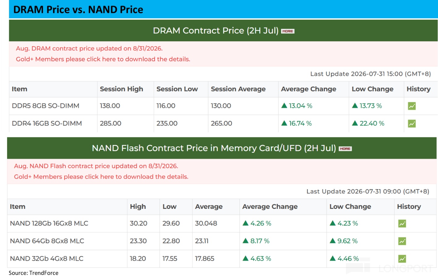
HBF is not yet in volume, so actual cost is uncertain, but its build mirrors HBM aside from NAND vs. DRAM dies. So the die‑level price gap offers a guide. TrendForce’s latest contracts show DRAM vs. NAND $/GB differs by over 8x, with DRAM (DDR5) at ~$16/GB and NAND (MLC) at ~$1.9/GB.
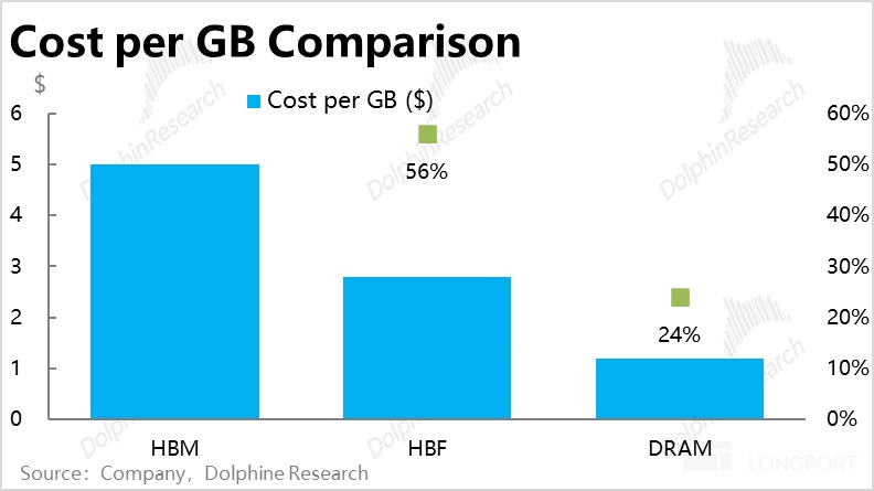
On manufacturing, third‑party estimates put HBM build cost near ~$5/GB recently and rising with spec, while commodity DRAM is under ~$1.2/GB and falling with mature processes. This aligns with HBM’s reported wafer loss at ~3–4x that of standard DRAM. For HBF, cheaper NAND dies are offset by similar stacking and packaging costs.
Company guidance suggests HBF build cost at ~3–4x that of commodity NAND, implying roughly ~$2.8/GB, or ~56% of HBM. Thus, on capacity, HBF can save nearly half the cost. But HBF essentially trades bandwidth for capacity, and its $/GB discount roughly matches its bandwidth deficit vs. HBM.
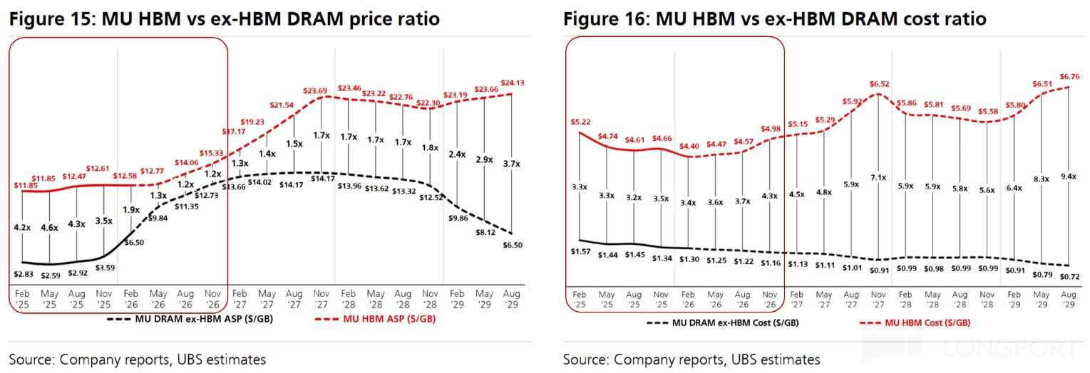
Another notable trend is that HBM costs about 4x commodity DRAM, yet the selling price gap is narrowing fast. In recent months, commodity DRAM prices have reached over 80% of HBM, and SK Hynix management said earlier this year that HBM GPM is only ~60% vs. ~80% for commodity DRAM. Lower‑cost, simpler DRAM has been more profitable.
HBM sells to a few big clients on long‑term pricing and lacks flexibility, while commodity DRAM sells to a fragmented base and can price to market. This validates our prior point that despite HBM’s complexity, memory makers capture less bargaining power and value because of customer concentration, though reports suggest new HBM contracts may rise from $15–17/GB to $20–30/GB, which would ease the margin gap. Pricing power dynamics remain in flux.
3.2 Capacity vs. bandwidth: which matters more
Back to HBF vs. HBM: if capacity is the priority, HBF offers better value; if bandwidth matters more, HBM is cheaper by an order of magnitude per unit of bandwidth. This supports the view that technology choices hinge on whether future bottlenecks are more about capacity or bandwidth. Capacity bottlenecks favor back‑row memory and HBF; bandwidth bottlenecks force maximizing front‑row performance or scaling interconnects, at higher cost.
What scenarios tilt toward capacity or bandwidth constraints. Capacity‑led scenarios include steadier model parameter growth (not a leap from the ~10T to ~100T range), with demand driven by higher user penetration, longer contexts, or more execution tasks that do not require inference. Bandwidth‑led scenarios involve continued rapid growth in total parameters and activations, longer chains of thought and context during inference, and tighter user latency expectations.
3.3 Three scenarios: who is the bottleneck, who gains more
Scenario 1: model parameters stabilize, growth comes from users, context length, and Agent execution, i.e., capacity grows faster. Technically, HBM layers and bandwidth need not jump, and added capacity shifts to back‑row memory, commodity DDR, and HBF, accelerating tiered hybrid architectures. Here, process difficulty fades and the issue becomes supply‑demand, taking memory back to a commodity logic where price tracks supply and demand, with unit cost and prices drifting down as capacity expands after 2027 and processes mature.
Beneficiaries are those with large, efficient capacity and the NAND chain (HBF, enterprise SSDs) serving capacity add‑ons. But it is the most cyclical of the three: once new capacity, including new entrants like CXMT, floods in, price pressure is largest and memory makers’ excess profit is hardest to sustain. Cyclicality would dominate returns.
Scenario 2: bandwidth is the main bottleneck and value spills over to packaging and foundry. This corresponds to higher bandwidth needs with rapid growth in parameters and activations, longer reasoning chains, and higher generation speed demands. Layers may not keep rising and could even drop with more stacks, shifting competition from stacking to Base Die signaling, interposer routing, and 3D packaging, putting the choke point on TSMC’s CoWoS and advanced‑node Base Die capacity.
Total memory system cost and scarcity likely keep climbing, but more of the scarcity premium accrues to packaging and foundry. Base Dies are increasingly custom‑designed by customers and fabbed by TSMC, HBM becomes further customized, and memory makers look more like die suppliers tied closely to a few big clients. TSMC benefits most, while among memory makers, Samsung can offer integrated Base Die and packaging 'one‑stop' solutions.
Scenario 3: both capacity and bandwidth are tight, a 'super‑cycle' for memory. Parameters step up again (e.g., from ~10T to ~100T) while users and context keep expanding. Technically, all paths must advance: stack heights likely rise and bandwidth must scale, lifting memory scarcity and prices the most and straining both DRAM wafers and packaging, with DRAM wafer adds slower and becoming the hardest constraint.
Both memory and packaging capture more value, and compared with Scenario 2, memory makers regain bargaining power because yields and bonding for high‑layer stacks are controlled by them. Note the scenarios are not mutually exclusive: training and frontier inference are bandwidth‑hungry, while large‑scale Agent inference is capacity‑hungry, and NVIDIA, AMD, and ASICs may choose different HBM configs. Reality will likely be a mix under a tiered hybrid architecture, with only the dominant share in question.
3.4 Closing
On capacity, stacking higher with thinner dies and advanced bonding places every added GB on the front‑row HBM’s fast lanes, but at the cost of process difficulty, yield, and DRAM wafer burn. Spreading more stacks over more area via multi‑row memory, HBF, or more low‑layer stacks lowers process demands and unit cost but either sacrifices bandwidth or shifts pressure to Base Dies and CoWoS capacity. On bandwidth, there is no shortcut: width and rate constrain each other, and big gains require grinding on Base Dies, interposers, and 3D packaging, much of which sit outside memory makers’ direct control.
The path taken hinges on whether AI demand is bottlenecked by capacity or bandwidth. If capacity, memory reverts to a volume game where capacity and cost decide winners; if bandwidth, packaging and foundry gain voice and memory makers’ bargaining power could be diluted. If both are tight, memory process and capacity become the hardest constraints and memory makers weigh most in the chain.
Dolphin Research currently sees capacity needs as the highest‑certainty trend, with users, usage, and Agent penetration likely to keep rising. The key ahead is the slope of model parameter growth, which will set the required pace of bandwidth gains. Signals to watch include:
i) HBM layer counts and stack counts ultimately adopted by NVIDIA, AMD, and ASIC vendors; ii) actual HBM4E operating rates and the rollout cadence for HBM5’s doubled width; iii) relative expansion of CoWoS vs. DRAM wafers; iv) first HBF adoptions around 2027.
With this, Dolphin Research has mapped the memory technology landscape, and the divergent routes will ultimately play out at the company level. The next piece will pivot from tech to supply‑demand, from industry to company, assessing vendor‑client lock‑in and likely financial trajectories to see who can win. Stay tuned.
<End of full text>
Related articles:
'Memory Is the New Compute: Why HBM Stands Out'
Risk disclosure and statement: Dolphin Research Disclaimer and General Disclosure


The copyright of this article belongs to the original author/organization.
The views expressed herein are solely those of the author and do not reflect the stance of the platform. The content is intended for investment reference purposes only and shall not be considered as investment advice. Please contact us if you have any questions or suggestions regarding the content services provided by the platform.